|
|
|
PDF ZNBG3118 Data sheet ( Hoja de datos )
| Número de pieza | ZNBG3118 | |
| Descripción | A Flexible Bias And Control Solution | |
| Fabricantes | Zetex Semiconductors | |
| Logotipo | ||
Hay una vista previa y un enlace de descarga de ZNBG3118 (archivo pdf) en la parte inferior de esta página. Total 10 Páginas | ||
|
No Preview Available !
A Product Line of
Diodes Incorporated
ZNBG3118
LNA GaAs FET BIAS CONTROLLER WITH POLARIZATION AND BAND SELECT
Summary
The ZNBG3118 is a bias and control solution designed for Satellite Low Noise Blocks (LNB’s). Providing three bias stages to
power control and protect the GaAs or HEMT FET low noise amplifier’s (LNA’s). The ZNBG3118 integrates an accurate voltage
detector to select the LNB polarisation channel and an advanced tone detector to select the local oscillator (LO) for band
switching.
Features
• Provides bias for up to three GaAs and HEMT FETs
• Dynamic FET protection and temperature compensation
• Drain current set by external resistor
• Regulated negative rail generator requires only 2 external
capacitors
• Accurate voltage detector and polarisation switch for
LNB’s
• 22kHz tone detection for band switching with rejection of
unwanted signals
• Band switch supports both Discrete, MIMIC and PLL
local oscillators
• Compliant with ASTRA control specifications
• Low current for power efficient systems
• Wide operating supply range of 3.3V to 8V
Pin Assignments
G1
GND
CNB1
CNB2
Top View
CSUB
LB
HB
VCC
LOV
Application
• Single Output LNB’s
• Two single type twin LNB’s
• Low power LNB’s
www.DataSheet4U.com
• PLL Single LNB’s
Bottom View
Single Universal LNB System Diagram
ZNBG3118
Document number: DS32049 Rev. 1 - 2
1 of 10
www.diodes.com
January 2010
© Diodes Incorporated
1 page 
A Product Line of
Diodes Incorporated
Typical Characteristics (Measured at TAMB = 25°C, VCC = 5V, RCAL = 39k (setting ID to 10mA) unless otherwise stated)
ZNBG3118
16
14
12
10
8
6
4
2
0
0 20 40 60 80 100 120 140 160 180 200
RCAL Value (kΩ )
Drain Current vs RCAL Value
2.5
2.4
2.3
2.2
2.1
2
1.9
1.8
1.7
1.6
1.5
0 2 4 6 8 10 12 14
Drain Current (mA)
Drain Voltage vs Drain Current
16
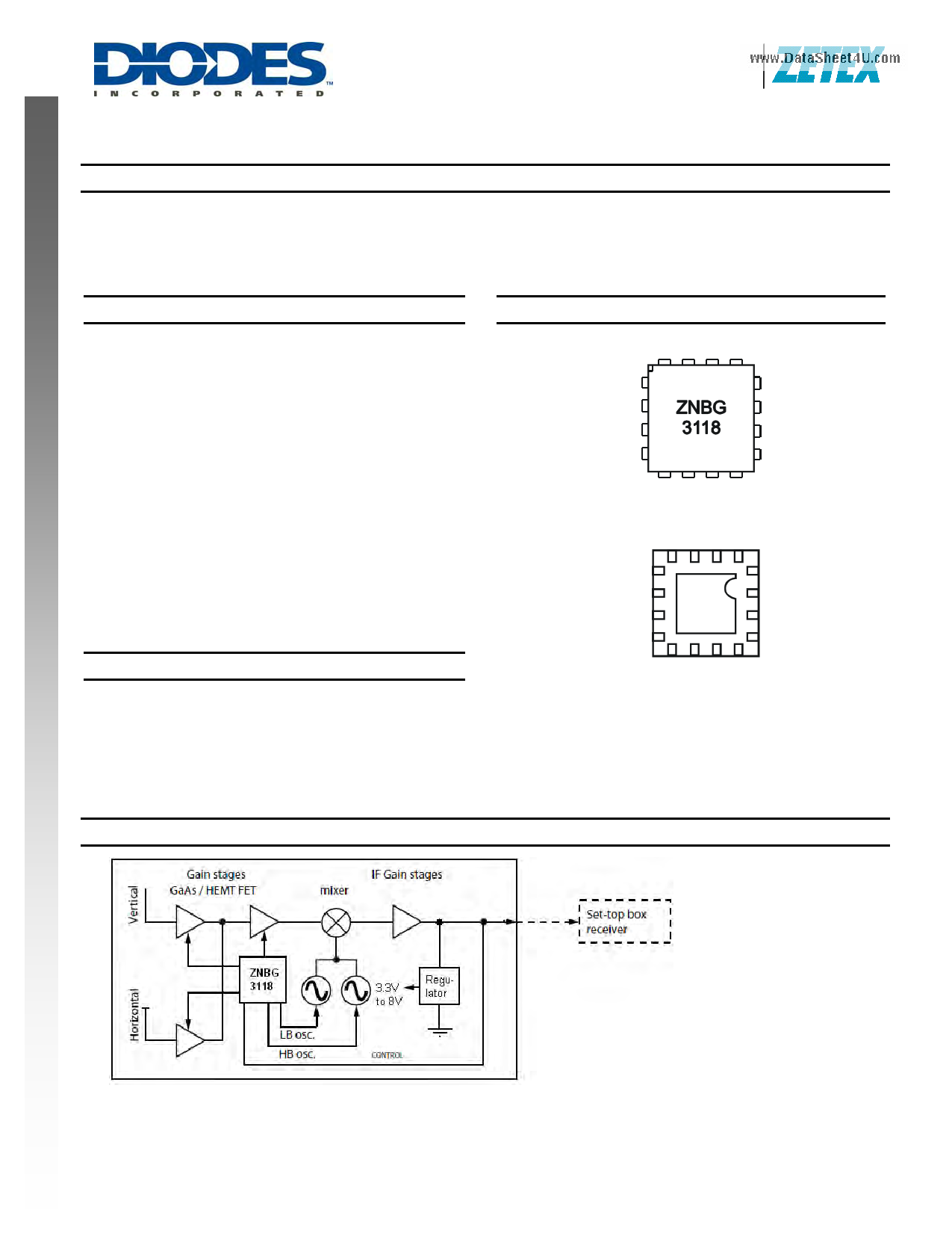
Single Universal Block Diagram
Figure 1 shows the main elements of a typical single universal LNB. The ZNBG3118 is compliant with virtually all markets including
the fleet of Astra satellites. The simple but flexible solution provides the negative rail, FET bias control, polarisation switch control,
tone detection and band switching with the minimum of external components. The ZNBG3118 can be also used in other DBS
applications such a twin output, mono-block and Low power LNB’s.
www.DataSheet4U.com
Figure 1 Typical single universal LNB system diagram
Polarization and band switching on the ZNBG3118 uses the standard 13V-17V and 22kHz as defined by Astra. The exception is
that the devices voltage detector has a much tighter tolerance than defined to increase field reliability. The tone detector has been
designed to cope with distorted 22kHz tones so reliability is maintained with regional differences and variations on set-top box
designs.
Tone detection and band switching has been designed to meet various different system architectures. The following diagrams
(figures 2 to 4) show how this feature operates in an LNB and the external components required. The presence or absence of a
22kHz tone applied to pin FIN enables one of two outputs, LB and HB. A tone present enables HB and tone absent enables LB.
The LB and HB outputs are designed to be compatible with MMIC, Discrete (bipolar or FET) and PLL based local oscillator
applications and are easily configured by the LOV pin.
Bi-polar or FET local oscillators
Referring to Figure 2 wiring pin LOV to a positive voltage source (e.g. a potential divider across VCC and ground set to the required
oscillator supply voltage, VOSC) will force the LB and HB outputs to provide the required oscillator supply. VOSC when enabled and
0V when disabled. Driving loads of up to 35mA, the maximum allowed programmed output voltage of LB and HB is VCC -1V. If a
greater supply voltage is required for the oscillators then it may be possible to use an oscillator circuit.
ZNBG3118
Document number: DS32049 Rev. 1 - 2
5 of 10
www.diodes.com
January 2010
© Diodes Incorporated
5 Page | ||
| Páginas | Total 10 Páginas | |
| PDF Descargar | [ Datasheet ZNBG3118.PDF ] | |
Hoja de datos destacado
| Número de pieza | Descripción | Fabricantes |
| ZNBG3110 | FET BIAS CONTROLLER WITH POLARISATION SWITCH AND TONE DETECTION | Zetex Semiconductors |
| ZNBG3111 | FET BIAS CONTROLLER WITH POLARISATION SWITCH AND TONE DETECTION | Zetex Semiconductors |
| ZNBG3113 | FET BIAS CONTROLLER WITH POLARISATION SWITCH AND TONE DETECTION | Zetex Semiconductors |
| ZNBG3114 | FET BIAS CONTROLLER WITH POLARISATION SWITCH AND TONE DETECTION | Zetex Semiconductors |
| Número de pieza | Descripción | Fabricantes |
| SLA6805M | High Voltage 3 phase Motor Driver IC. |
Sanken |
| SDC1742 | 12- and 14-Bit Hybrid Synchro / Resolver-to-Digital Converters. |
Analog Devices |
|
DataSheet.es es una pagina web que funciona como un repositorio de manuales o hoja de datos de muchos de los productos más populares, |
| DataSheet.es | 2020 | Privacy Policy | Contacto | Buscar |