|
|
|
PDF P75NF75 Data sheet ( Hoja de datos )
| Número de pieza | P75NF75 | |
| Descripción | STP75NF75 | |
| Fabricantes | STMicroelectronics | |
| Logotipo | ||
 1. Power MOSFET ( PDF ) Hay una vista previa y un enlace de descarga de P75NF75 (archivo pdf) en la parte inferior de esta página. Total 16 Páginas | ||
|
No Preview Available !
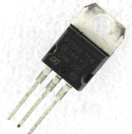
STB75NF75
STP75NF75 - STP75NF75FP
N-channel 75V - 0.0095Ω - 80A - TO-220 - TO-220FP - D2PAK
STripFET™ II Power MOSFET
General features
Type
STB75NF75
STP75NF75
STP75NF75FP
VDSS
75V
75V
75V
RDS(on)
<0.011Ω
<0.011Ω
<0.011Ω
ID
80A(1)
80A(1)
80A(1)
1. Current limited by package
■ Exceptional dv/dt capability
■ 100% avalanche tested
Description
This Power MOSFET series realized with
STMicroelectronics unique STripFET™ process
has specifically been designed to minimize input
capacitance and gate charge. It is therefore
suitable as primary switch in advanced high-
efficiency, high-frequency isolated DC-DC
converters for Telecom and Computer
applications. It is also intended for any
applications with low gate drive requirements.
Applications
www.DataSheet4U.com
■ Switching application
3
2
1
TO-220
3
2
1
TO-220FP
3
1
D²PAK
Internal schematic diagram
Order codes
Part number
STB75NF75T4
STP75NF75
STP75NF75FP
February 2007
Marking
B75NF75
P75NF75
P75NF75
Rev 8
Package
D²PAK
TO-220
TO-220FP
Packaging
Tape & reel
Tube
Tube
1/16
www.st.com
16
1 page 
STB75NF75 - STP75NF75 - STP75NF75FP
Electrical characteristics
Table 5. Switching times
Symbol
Parameter
td(on)
tr
td(off)
tf
Turn-on delay time
Rise time
Turn-off delay time
Fall time
Test conditions
VDD= 37.5V, ID= 45A,
RG=4.7Ω, VGS=10V
Figure 15 on page 9
Min. Typ. Max. Unit
25 ns
100 ns
66 ns
30 ns
Table 6. Source drain diode
Symbol
Parameter
Test conditions
Min Typ. Max Unit
ISD
ISDM(1)
VSD(2)
Source-drain current
Source-drain current (pulsed)
Forward on voltage
trr
Qrr
IRRM
Reverse recovery time
Reverse recovery charge
Reverse recovery current
ISD = 80A, VGS = 0
ISD = 80A,
di/dt = 100A/µs,
VDD = 25V, TJ = 150°C
Figure 17 on page 9
80 A
320 A
1.5 V
132 ns
660 nC
10 A
1. Pulse width limited by safe operating area
2. Pulsed: pulse duration=300µs, duty cycle 1.5%
www.DataSheet4U.com
5/16
5 Page 
STB75NF75 - STP75NF75 - STP75NF75FP
Package mechanical data
DIM.
A
b
b1
c
D
E
e
e1
F
H1
J1
L
L1
L20
L30
øP
Q
MIN.
4.40
0.61
1.15
0.49
15.25
10
2.40
4.95
1.23
6.20
2.40
13
3.50
3.75
2.65
TO-220 MECHANICAL DATA
mm.
TYP
16.40
28.90
MAX.
4.60
0.88
1.70
0.70
15.75
10.40
2.70
5.15
1.32
6.60
2.72
14
3.93
3.85
2.95
MIN.
0.173
0.024
0.045
0.019
0.60
0.393
0.094
0.194
0.048
0.244
0.094
0.511
0.137
0.147
0.104
inch
TYP.
0.645
1.137
MAX.
0.181
0.034
0.066
0.027
0.620
0.409
0.106
0.202
0.052
0.256
0.107
0.551
0.154
0.151
0.116
www.DataSheet4U.com
11/16
11 Page | ||

| Páginas | Total 16 Páginas | |
| PDF Descargar | [ Datasheet P75NF75.PDF ] | |
Hoja de datos destacado
| Número de pieza | Descripción | Fabricantes |
| P75NF75 | STP75NF75 | STMicroelectronics |
| Número de pieza | Descripción | Fabricantes |
| SLA6805M | High Voltage 3 phase Motor Driver IC. |
Sanken |
| SDC1742 | 12- and 14-Bit Hybrid Synchro / Resolver-to-Digital Converters. |
Analog Devices |
|
DataSheet.es es una pagina web que funciona como un repositorio de manuales o hoja de datos de muchos de los productos más populares, |
| DataSheet.es | 2020 | Privacy Policy | Contacto | Buscar |