|
|
|
PDF MAX11045 Data sheet ( Hoja de datos )
| Número de pieza | MAX11045 | |
| Descripción | (MAX11044 - MAX11046) Simultaneous-Sampling ADCs | |
| Fabricantes | Maxim Integrated Products | |
| Logotipo | ||
Hay una vista previa y un enlace de descarga de MAX11045 (archivo pdf) en la parte inferior de esta página. Total 19 Páginas | ||
|
No Preview Available !
19-5036; Rev 0; 10/09
EVAALVUAAILTAIOBNLEKIT
4-/6-/8-Channel, 16-Bit,
Simultaneous-Sampling ADCs
General Description
The MAX11044/MAX11045/MAX11046† 16-bit ADCs
offer 4, 6, or 8 independent input channels. Featuring
independent track and hold (T/H) and SAR circuitry,
these parts provide simultaneous sampling at 250ksps
for each channel.
The MAX11044/MAX11045/MAX11046 accept a ±5V
input. All inputs are overrange protected with internal
±20mA input clamps providing overrange protection
with a simple external resistor. Other features include a
4MHz T/H input bandwidth, internal clock, and internal
or external reference. A 20MHz, 16-bit, bidirectional,
parallel interface provides the conversion results and
accepts digital configuration inputs.
The MAX11044/MAX11045/MAX11046 operate with a
4.75V to 5.25V analog supply and a separate flexible 2.7V
to 5.25V digital supply for interfacing with the host without a
level shifter. The MAX11044/MAX11045/MAX11046
are available in a 56-pin TQFN package and operate over
the extended -40°C to +85°C temperature range.
Applications
Automatic Test Equipment
Power-Factor Monitoring and Correction
Power-Grid Protection
Multiphase Motor Control
Vibration and Waveform Analysis
†Patent pending.
www.DataSheet4U.com
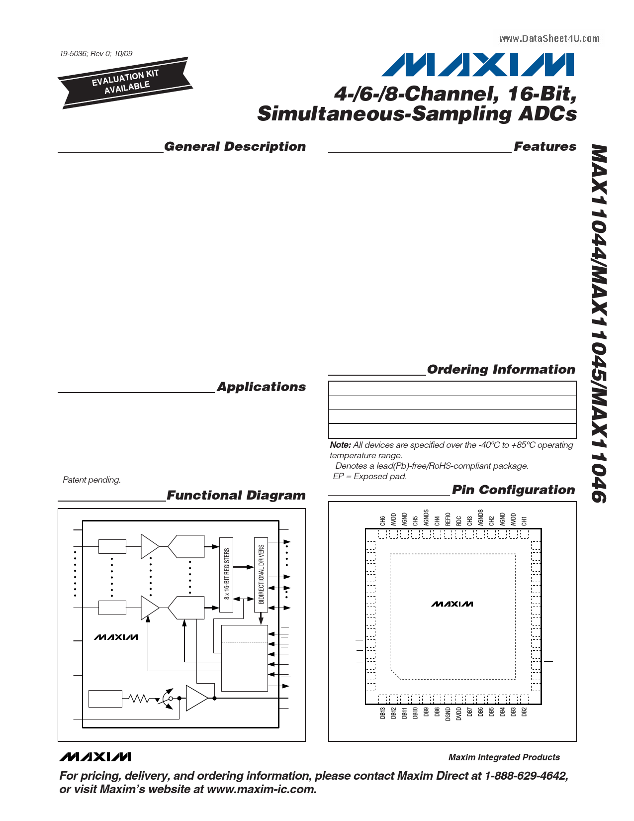
Functional Diagram
AVDD
CH0
CLAMP S/H 16-BIT ADC
CH7
CLAMP S/H 16-BIT ADC
AGNDs
AGND
MAX11044
MAX11045
MAX11046
REFIO
BANDGAP
REFERENCE
INT REF
EXT REF
REF
BUF
DVDD
DB15
DB4
DB3
DB0
CONFIGURATION
REGISTERS
INTERFACE
AND
CONTROL
WR
RD
CS
CONVST
SHDN
EOC
RDC
DGND
Features
♦ 4-/6-/8-Channel 16-Bit ADC
♦ Single Analog and Digital Supply
♦ High-Impedance Inputs Up to 1GΩ
♦ On-Chip T/H Circuit for Each Channel
♦ Fast 3µs Conversion Time
♦ High Throughput: 250ksps for All 8 Channels
♦ 16-Bit, High-Speed, Parallel Interface
♦ Internal Clocked Conversions
♦ 10ns Aperture Delay
♦ 100ps Channel-to-Channel T/H Matching
♦ Low Drift, Accurate 4.096V Internal Reference
Providing an Input Range of ±5V
♦ External Reference Range of 3.0V to 4.25V,
Allowing Full-Scale Input Ranges of ±4.0V to ±5.2V
♦ 56-Pin TQFN Package (8mm x 8mm)
♦ Evaluation Kit Available
Ordering Information
PART
PIN-PACKAGE
CHANNELS
MAX11044ETN+
56 TQFN-EP*
4
MAX11045ETN+
56 TQFN-EP*
6
MAX11046ETN+
56 TQFN-EP*
8
Note: All devices are specified over the -40°C to +85°C operating
temperature range.
+Denotes a lead(Pb)-free/RoHS-compliant package.
*EP = Exposed pad.
Pin Configuration
TOP VIEW
42 41 40 39 38 37 36 35 34 33 32 31 30 29
RDC 43
AGNDS 44
CH7 45
AGND 46
AVDD 47
AGNDS 48
RDC 49
DGND 50
DVDD 51
MAX11044
MAX11045
MAX11046
28 RDC
27 AGNDS
26 CH0
25 AGND
24 AVDD
23 AGNDS
22 RDC
21 DGND
20 DVDD
WR 52
CS 53
RD 54
DB15 55
DB14 56
+
19 SHDN
18 CONVST
17 EOC
*EP 16 DB0
15 DB1
1 2 3 4 5 6 7 8 9 10 11 12 13 14
TQFN
8mm x 8mm
________________________________________________________________ Maxim Integrated Products 1
For pricing, delivery, and ordering information, please contact Maxim Direct at 1-888-629-4642,
or visit Maxim’s website at www.maxim-ic.com.
1 page 
4-/6-/8-Channel, 16-Bit,
Simultaneous-Sampling ADCs
Typical Operating Characteristics
(AVDD = 5V, DVDD = 3.3V, TA = +25°C, fSAMPLE = 250ksps, internal reference, unless otherwise noted.)
INTEGRAL NONLINEARITY vs. CODE
1.0
0.8
0.6
0.4
0.2
0
-0.2 VAVDD = 5.25V
-0.4 VDVDD = 3.3V
-0.6
fSAMPLE = 250ksps
TA = +25°C
-0.8 VRDC = 4.096V
-1.0
OUTPUT CODE (DECIMAL)
DIFFERENTIAL NONLINEARITY vs. CODE
1.0
0.8
0.6
0.4
0.2
0
-0.2
-0.4 VAVDD = 5.25V
VDVDD = 3.3V
-0.6 fSAMPLE = 250ksps
-0.8
TA = +25°C
VRDC = 4.096V
-1.0
OUTPUT CODE (DECIMAL)
INL AND DNL
vs. ANALOG SUPPLY VOLTAGE
1.5
MAX INL
1.0
0.5
0 MIN DNL
MAX DNL
-0.5
-1.0
-1.5
4.75
MIN INL
VDVDD = 3.3V
fSAMPLE = 250ksps
TA = +25°C
VRDC = 4.096V
4.85 4.95 5.05 5.15 5.25
VAVDD (V)
INL AND DNL
vs. TEMPERATURE
1.5
MAX INL
1.0 MAX DNL
0.5
0
-0.5
www.DataSheet4U.com
-1.0
MIN DNL
MIN INL
VAVDD = 5.25V
VDVDD = 3.3V
fSAMPLE = 250ksps
VRDC = 4.096V
-1.5
-40
-15 10 35 60
TEMPERATURE (°C)
85
ANALOG SUPPLY CURRENT
vs. SUPPLY VOLTAGE
45
MAX11046 CONVERTING
TA = +25°C
fSAMPLE = 250ksps
40 MAX11046 STATIC
MAX11045 CONVERTING
35 MAX11045 STATIC
MAX11044 CONVERTING
30
MAX11044 STATIC
25
4.75 4.85 4.95 5.05 5.15 5.25
VAVDD (V)
ANALOG SUPPLY CURRENT
vs. TEMPERATURE
45
MAX11046 CONVERTING VAVDD = 5.0V
fSAMPLE = 250ksps
40 MAX11046 STATIC
MAX11045 CONVERTING
35 MAX11045 STATIC
MAX11044 CONVERTING
30
25
-40
MAX11044 STATIC
-15 10 35 60
TEMPERATURE (°C)
85
DIGITAL SUPPLY CURRENT
vs. SUPPLY VOLTAGE
12
TA = +25°C
10 fSAMPLE = 250ksps
MAX11046 CONVERTING
8
6
MAX11045 CONVERTING
4
MAX11044/MAX11045/
MAX11046 STATIC
2
MAX11044 CONVERTING
0
2.75 3.25 3.75 4.25 4.75 5.25
VDVDD (V)
_______________________________________________________________________________________ 5
5 Page 
4-/6-/8-Channel, 16-Bit,
Simultaneous-Sampling ADCs
To make use of the input clamps (see Figure 1), con-
nect a resistor (RS) between the analog input and the
voltage source to limit the voltage at the analog input so
that the fault current into the MAX11044/MAX11045/
MAX11046 does not exceed ±20mA. Note that the volt-
age at the analog input pin limits to approximately 7V
during a fault condition so the following equation can
be used to calculate the value of RS:
RS
=
VFAULT _ MAX
20mA
- 7V
where VFAULT_MAX is the maximum voltage that the
source produces during a fault condition.
Figures 2 and 3 illustrate the clamp circuit voltage-cur-
rent characteristics for a source impedance RS =
1280Ω. While the input voltage is within the ±(VAVDD +
300mV) range, no current flows in the input clamps.
Once the input voltage goes beyond this voltage range,
the clamps turn on and limit the voltage at the input pin.
www.DataSheet4U.com
INPUT
PIN
SIGNAL VOLTAGE
AVDD
RS
CH0
SOURCE
CLAMP
S/H 16-BIT ADC
CH7
CLAMP
S/H 16-BIT ADC
AGNDS
AGND
MAX11044
MAX11045
MAX11046
REFIO
BANDGAP
REFERENCE
INT REF
EXT REF
REF
BUF
DVDD
DB15
DB4
DB3
DB0
CONFIGURATION
REGISTERS
INTERFACE
AND
CONTROL
WR
RD
CS
CONVST
SHDN
EOC
RDC
DGND
Figure 1. Required Setup for Clamp Circuit
30
RS = 1280Ω
20 VAVDD = 5V
AT CH_ INPUT
10
0
AT SOURCE
30
RS = 1280Ω
20 VAVDD = 5V
10
AT SOURCE
0
AT CH_ INPUT
-10 -10
-20 -20
-30
-50 -30 -10 10 30 50
SIGNAL VOLTAGE AT SOURCE AND PIN (V)
Figure 2. Input Clamp Characteristics
-30
-8 -6 -4 -2 0 2 4 6 8
SIGNAL VOLTAGE AT SOURCE AND PIN (V)
Figure 3. Input Clamp Characteristics (Zoom In)
______________________________________________________________________________________ 11
11 Page | ||
| Páginas | Total 19 Páginas | |
| PDF Descargar | [ Datasheet MAX11045.PDF ] | |
Hoja de datos destacado
| Número de pieza | Descripción | Fabricantes |
| MAX1104 | 8-Bit CODECs | Maxim Integrated |
| MAX11040 | Sigma-Delta ADC | Maxim Integrated Products |
| MAX11040K | (MAX11040K / MAX11060) Sigma-Delta ADCs | Maxim Integrated Products |
| MAX11041 | (MAX11041 / MAX11042) Wired Remote Controllers | Maxim Integrated Products |
| Número de pieza | Descripción | Fabricantes |
| SLA6805M | High Voltage 3 phase Motor Driver IC. |
Sanken |
| SDC1742 | 12- and 14-Bit Hybrid Synchro / Resolver-to-Digital Converters. |
Analog Devices |
|
DataSheet.es es una pagina web que funciona como un repositorio de manuales o hoja de datos de muchos de los productos más populares, |
| DataSheet.es | 2020 | Privacy Policy | Contacto | Buscar |