|
|
|
PDF TC7MPH3125FTG Data sheet ( Hoja de datos )
| Número de pieza | TC7MPH3125FTG | |
| Descripción | Low Voltage/Low Power 2-Bit X 2 Dual Supply Bus Transceiver | |
| Fabricantes | Toshiba Semiconductor | |
| Logotipo | ||
Hay una vista previa y un enlace de descarga de TC7MPH3125FTG (archivo pdf) en la parte inferior de esta página. Total 23 Páginas | ||
|
No Preview Available !
TC7MPH3125FK/FTG
TOSHIBA Digital Integrated Circuit Silicon Monolithic
TC7MPH3125FK,TC7MPH3125FTG
Low Voltage/Low Power 2-Bit × 2 Dual Supply Bus Transceiver with Bushold
The TC7MPH3125FK/FTG is a dual supply, advanced
high-speed CMOS 4-bit dual supply voltage interface bus
transceiver fabricated with silicon gate CMOS technology.
Designed for use as an interface between a 1.2-V, 1.5-V, 1.8-V,
or 2.5-V bus and a 1.8-V, 2.5-V or 3.6-V bus in mixed 1.2-V, 1.5-V,
1.8-V or 2.5-V/1.8-V, 2.5-V or 3.6-V supply systems.
The A-port interfaces with the 1.2-V, 1.5-V, 1.8-V or 2.5-V bus,
the B-port with the 1.8-V, 2.5-V, 3.3-V bus.
The direction of data transmission is determined by the level of
the DIR input. The enable input (OE) can be used to disable the
device so that the buses are effectively isolated. The bus of a B
bus side at floating state is maintained in an appropriate logic
level due to a bushold circuit to a B bus. Moreover, the bushold
circuit which is added to a B bus is off when OE is low.
All inputs are equipped with protection circuits against static
discharge or transient excess voltage.
TC7MP3125FK
TC7MP3125FTG
Features
• Bidirectional interface between 1.2-V and 1.8-V, 1.2-V and
2.5-V, 1.2-V and 3.3-V, 1.5-V and 2.5-V, 1.5-V and 3.3-V, 1.8-V
and 2.5-V, 1.8-V and 3.3-V or 2.5-V and 3.3-V buses.
• High-speed operation: tpd = 6.8 ns (max) (VCCA = 2.5 ± 0.2 V,
VCCB = 3.3 ± 0.3 V)
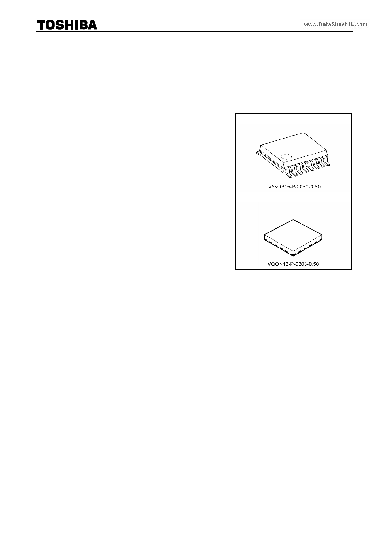
Weight
VSSOP16-P-0030-0.50: 0.02 g (typ.)
VQON16-P-0303-0.50: 0.013 g (typ.)
tpd = 8.9 ns (max) (VCCA = 1.8 ± 0.15 V, VCCB = 3.3 ± 0.3 V)
tpd = 10.3 ns (max) (VCCA = 1.5 ± 0.1 V, VCCB = 3.3 ± 0.3 V)
tpd = 61 ns (max) (VCCA = 1.2 ± 0.1 V, VCCB = 3.3 ± 0.3 V)
www.DataSheet4U.com
tpd = 9.5 ns (max) (VCCA = 1.8 ± 0.15 V, VCCB = 2.5 ± 0.2 V)
tpd = 10.8 ns (max) (VCCA = 1.5 ± 0.15 V, VCCB = 2.5 ± 0.2 V)
tpd = 60 ns (max) (VCCA = 1.2 ± 0.15 V, VCCB = 2.5 ± 0.2 V)
tpd = 58 ns (max) (VCCA = 1.2 ± 0.1 V, VCCB = 1.8 ± 0.15 V)
• Output current: IOH/IOL = ±12 mA (min) (VCC = 3.0 V)
IOH/IOL = ±9mA (min) (VCC = 2.3 V)
IOH/IOL = ±3 mA (min) (VCC = 1.65 V)
IOH/IOL = ±1mA (min) (VCC = 1.4 V)
• Latch-up performance: ±300 mA
• ESD performance: Machine model ≥ ±200 V
Human body model ≥ ±2000 V
• Ultra-small package: VSSOP (US16), VQON16
• Bushold circuit is build in only the B bus side. (Only in OE = “H”, a former state is maintained.)
• Low current consumption: Using the new circuit significantly reduces current consumption when OE = “H”.
Suitable for battery-driven applications such as PDAs and cellular phones.
• Floating A-bus and B-bus are permitted. (when OE = “H”)
• 3.6-V tolerant function provided on A-bus terminal, DIR and OE terminal.
Note 1: Do not apply a signal to any bus pins when it is in the output mode. Damage may result.
Note: When mounting VQON package, the type of recommended flux is RA or RMA.
1
2007-10-19
1 page 
Operating Ranges (Note 1)
TC7MPH3125FK/FTG
Characteristics
Symbol
Rating
Unit
Power supply voltage
Input voltage
(DIR, OE )
Bus I/O voltage
(Note 2)
VCCA
VCCB
VIN
VI/OA
VI/OB
Output current
IOUTA
IOUTB
Operating temperature
Input rise and fall time
Topr
dt/dv
1.1 to 2.7
1.65 to 3.6
V
0 to 3.6
V
0 to 3.6 (Note 3)
0 to VCCA (Note 4)
0 to VCCB (Note 4)
±9 (Note 5)
±3 (Note 6)
±1 (Note 7)
±12 (Note 8)
±9 (Note 9)
±3 (Note 10)
−40 to 85
0 to 10 (Note 11)
V
mA
°C
ns/V
Note 1:
The operating ranges must be maintained to ensure the normal operation of the device. Unused inputs and
bus inputs must be tied to either VCC or GND. Please connect both bus inputs and the bus outputs with
VCC or GND when the I/O of the bus terminal changes by the function. In this case, please note that the
output is not short-circuited.
Note 2: Don’t use in VCCA > VCCB
Note 3: Output in OFF state
Note 4: High or low state
Note 5: VCCB= 2.3 to 2.7 V
Note 6: VCCB = 1.65 to 1.95 V
www.DataShNeoette4U7.:comVCCB = 1.4 to 1.6 V
Note 8: VCCA = 3.0 to 3.6 V
Note 9: VCCA = 2.3 to 2.7 V
Note 10: VCCA = 1.65 to 1.95 V
Note 11: VIN = 0.8 to 2.0 V, VCCA = 2.5 V, VCCB = 3.0 V
5 2007-10-19
5 Page 
TC7MPH3125FK/FTG
DC Characteristics (1.4 V ≤ VCCA < 1.65 V, 2.3 V ≤ VCCB ≤ 2.7 V)
Characteristics
Symbol
Test Condition
Ta = −40 to 85°C
VCCA (V) VCCB (V)
Unit
Min Max
H-level input voltage
L-level input voltage
H-level output voltage
L-level output voltage
3-state output OFF state current
Input leakage current
Bushold input minimum drive hold
current
Bushold input over-drive current
to change state
VIHA
VIHB
VILA
VILB
VOHA
VOHB
VOLA
VOLB
IOZA
IOZB
IIN
IIHOLD
IIOD
DIR, OE , An
1.4 to 1.65 2.3 to 2.7
Bn 1.4 to 1.65 2.3 to 2.7
DIR, OE , An
1.4 to 1.65 2.3 to 2.7
Bn 1.4 to 1.65 2.3 to 2.7
IOHA = −100 μA 1.4 to 1.65 2.3 to 2.7
VIN = VIH or VIL IOHA = −1 mA
1.4 2.3 to 2.7
IOHB = −100 μA 1.4 to 1.65 2.3 to 2.7
IOHB = −9 mA 1.4 to 1.65 2.3
IOLA = 100 μA 1.4 to 1.65 2.3 to 2.7
VIN = VIH or VIL IOLA = 1 mA
IOLB = 100 μA
IOLB = 9mA
VIN = VIH or VIL
VOUT = 0 to 3.6 V
1.4 2.3 to 2.7
1.4 to 1.65 2.3 to 2.7
1.4 to 1.65 2.3
1.4 to 1.65 2.3 to 2.7
VIN = VIH or VIL
VOUT = 0 to 3.6 V
VIN (DIR, OE ) = 0 to 3.6 V
VIN = 0.7 V
VIN = 1.6 V
1.4 to 1.65 2.3 to 2.7
1.4 to 1.65 2.3 to 2.7
1.4 to 1.65 2.3
1.4 to 1.65 2.3
(Note 1) 1.4 to 1.65 2.7
(Note 2) 1.4 to 1.65 2.7
0.65 ×
VCCA
1.6
⎯
⎯
VCCA
− 0.2
1.05
VCCB
− 0.2
1.7
⎯
⎯
⎯
⎯
⎯
⎯
⎯
45
-45
⎯
⎯
⎯
⎯
0.30 ×
VCCA
0.7
⎯
⎯
⎯
⎯
0.2
0.35
0.2
0.6
±2.0
±2.0
±1.0
⎯
⎯
450
-450
V
V
V
V
μA
μA
μA
μA
www.DataShPeoewt4eUr-o.cffolmeakage current
Quiescent supply current
IOFF1
IOFF2
IOFF3
ICCA
ICCB
ICCA
ICCB
VIN, VOUT = 0 to 3.6 V
VINA = VCCA or GND
VINB = VCCB or GND
VINA = VCCA or GND
VINB = VCCB or GND
VCCA ≤ (VIN, VOUT) ≤ 3.6 V
VCCB ≤ (VIN, VOUT) ≤ 3.6 V
0 0 ⎯ 2.0
1.4 to 1.65
0
⎯ 2.0 μA
1.4 to 1.65 Open ⎯ 2.0
1.4 to 1.65 2.3 to 2.7 ⎯
2.0
μA
1.4 to 1.65 2.3 to 2.7 ⎯
2.0
1.4 to 1.65 2.3 to 2.7 ⎯ ±2.0
μA
1.4 to 1.65 2.3 to 2.7 ⎯ ±2.0
Note 1: An external driver must source at least the specified current to switch from LOW-to-HIGH.
Note 2: An external driver must sink at least the specified current to switch from HIGH-to-LOW.
11 2007-10-19
11 Page | ||
| Páginas | Total 23 Páginas | |
| PDF Descargar | [ Datasheet TC7MPH3125FTG.PDF ] | |
Hoja de datos destacado
| Número de pieza | Descripción | Fabricantes |
| TC7MPH3125FTG | Low Voltage/Low Power 2-Bit X 2 Dual Supply Bus Transceiver | Toshiba Semiconductor |
| Número de pieza | Descripción | Fabricantes |
| SLA6805M | High Voltage 3 phase Motor Driver IC. |
Sanken |
| SDC1742 | 12- and 14-Bit Hybrid Synchro / Resolver-to-Digital Converters. |
Analog Devices |
|
DataSheet.es es una pagina web que funciona como un repositorio de manuales o hoja de datos de muchos de los productos más populares, |
| DataSheet.es | 2020 | Privacy Policy | Contacto | Buscar |