|
|
|
PDF FDMF6704A Data sheet ( Hoja de datos )
| Número de pieza | FDMF6704A | |
| Descripción | High Frequency DrMOS Module | |
| Fabricantes | Fairchild Semiconductor | |
| Logotipo | ||
Hay una vista previa y un enlace de descarga de FDMF6704A (archivo pdf) en la parte inferior de esta página. Total 12 Páginas | ||
|
No Preview Available !
September 2008
FDMF6704A - XSTM DrMOS
tm
The Xtra Small High Performance, High Frequency DrMOS Module
Benefits
Ultra compact size - 6 mm x 6 mm MLP, 44 % space
saving compared to conventional MLP 8 mm x 8 mm
DrMOS packages.
Fully optimized system efficiency.
Clean voltage waveforms with reduced ringing.
High frequency operation.
Features
Ultra- compact thermally enhanced 6 mm x 6 mm MLP
package 84 % smaller than conventional discrete solutions.
Synchronous driver plus FET multichip module.
High current handling of 35 A.
Over 93 % peak efficiency.
Logic level PWM input.
Fairchild's PowerTrench® 5 technology MOSFETs for clean
voltage waveforms and reduced ringing.
Optimized for high switching frequencies of up to 1 MHz.
Skip mode SMOD [low side gate turn off] input.
Fairchild SyncFETTM [integrated Schottky diode] technology
in the low side MOSFET.
Integrated bootstrap Schottky diode.
Adaptive gate drive timing for shoot-through protection.
Driver output disable function [DISB# pin].
Undervoltage lockout (UVLO).
Fairchild Green Packaging and RoHS
compliant. Low profile SMD package.
www.DataSheet4U.com
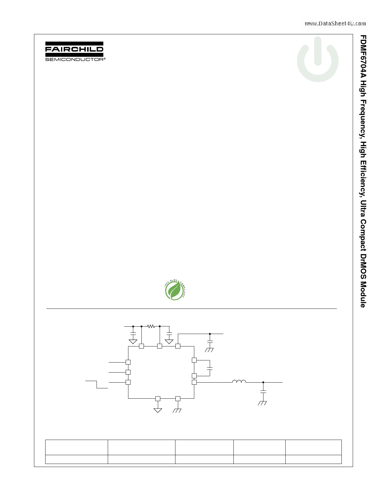
Power Train Application Circuit
5V
CVDRV
CVCIN
DISB#
PWM Input
OFF
ON
VDRV VCIN
DISB#
VIN
BOOT
PWM
SMOD#
PHASE
VSWH
CGND PGND
General Description
The XSTM DrMOS family is Fairchild’s next-generation fully-
optimized ultra-compact integrated MOSFET plus driver power
stage solution for high current, high frequency synchronous
buck DC-DC applications. The FDMF6704A DrMOS integrates
a driver IC, two power MOSFETs and a bootstrap Schottky
diode into a thermally enhanced compact 6 mm x 6 mm MLP
package. With an integrated approach, the complete switching
power stage is optimized with regards to driver and MOSFET
dynamic performance, system inductance and RDS(ON). This
greatly reduces the package parasitics and layout challenges
associated with conventional discrete solutions. The driver IC
incorporates advanced features such as SMOD. A 5 V gate
drive and an improved PCB interface [Low Side MOSFET
exposed pad] ensure higher performance. This product meets
the Intel 6 mm x 6 mm DrMOS pinout.
Applications
Compact blade servers V-core, non V-core and VTT DC-DC
converters.
Desktop computers V-core, non V-core and VTT DC-DC
converters.
Workstations V-core, non V-core and VTT DC-DC
converters.
Gaming Motherboards V-core, non V-core and VTT DC-DC
converters.
Gaming consoles.
High-current DC-DC Point of Load (POL) converters.
Networking and telecom microprocessor voltage regulators.
Small form factor voltage regulator modules.
12 V
CVIN
CBOOT
OUTPUT
COUT
Ordering Information
Figure 1. Power Train Application Circuit
Part
FDMF6704A
Current Rating @ 350 kHz
[A]
35
Input Voltage Typical
[V]
8-14
Frequency Max
[kHz]
1000
©2008 Fairchild Semiconductor Corporation
FDMF6704A Rev. C
1
Device
Marking
FDMF6704A
www.fairchildsemi.com
1 page 
Description of Operation
Circuit Description
The FDMF6704A is a driver plus FET module optimized for
synchronous buck converter topology. A single PWM input
signal is all that is required to properly drive the high-side and
the low-side MOSFETs. Each part is capable of driving speeds
up to 1 MHz.
Low-Side Driver
The low-side driver (LDRV) is designed to drive a ground
referenced low RDS(ON) N-channel MOSFET. The bias for LDRV
is internally connected between VDRV and CGND. When the
driver is enabled, the driver's output is 180° out of phase with
the PWM input. When the driver is disabled (DISB = 0 V), LDRV
is held low.
High-Side Driver
The high-side driver (HDRV) is designed to drive a floating
N-channel MOSFET. The bias voltage for the high-side driver is
developed by a bootstrap supply circuit, consisting of the
internal diode and external bootstrap capacitor (CBOOT). During
start-up, VSWH is held at PGND, allowing CBOOT to charge to
VDRV through the internal diode. When the PWM input goes
high, HDRV will begin to charge the high-side MOSFET's gate
(Q1). During this transition, charge is removed from CBOOT and
delivered to Q1's gate. As Q1 turns on, VSWH rises to VIN,
forcing the BOOT pin to VIN +VC(BOOT), which provides
sufficient VGS enhancement for Q1. To complete the switching
cycle, Q1 is turned off by pulling HDRV to VSWH. CBOOT is then
recharged to VDRV when VSWH falls to PGND. HDRV output is
in phase with the PWM input. When the driver is disabled, the
high-side gate is held low.
SMOD
The SMOD (Skip Mode) function allows for higher converter
efficiency under light load conditions. During SMOD, the LS
FET is disabled and it prevents discharging of output caps.
When the SMOD# pin is pulled high, the sync buck converter
www.DataSheet4U.com
PWM Input
DrvL
DrvLLOW
tDTHH
90 %
1V
will work in synchronous mode. When the SMOD# pin is pulled
low, the LS FET is turned off. The SMOD function does not have
internal current sensing. This SMOD# pin is connected to a
PWM controller which enables or disables the SMOD
automatically when the controller detects light load condition.
Normally this pin is Active Low.
Adaptive Gate Drive Circuit
The driver IC embodies an advanced design that ensures
minimum MOSFET dead-time while eliminating potential
shoot-through (cross-conduction) currents. It senses the state of
the MOSFETs and adjusts the gate drive, adaptively, to ensure
they do not conduct simultaneously. Refer to Figure 4 for the
relevant timing waveforms.
To prevent overlap during the low-to-high switching transition
(Q2 OFF to Q1 ON), the adaptive circuitry monitors the voltage
at the LDRV pin. When the PWM signal goes HIGH, Q2 will
begin to turn OFF after some propagation delay (tPDLL). Once
the LDRV pin is discharged below 1 V, Q1 begins to turn ON
after adaptive delay tDTHH.
To preclude overlap during the high-to-low transition (Q1 OFF to
Q2 ON), the adaptive circuitry monitors the voltage at the
VSWH pin. When the PWM signal goes LOW, Q1 will begin to
turn OFF after some propagation delay (tPDHL). Once the
VSWH pin falls below 1 V, Q2 begins to turn ON after adaptive
delay tDTLH.
Additionally, VGS of Q1 is monitored. When VGS(Q1) is
discharged low, a secondary adaptive delay is initiated, which
results in Q2 being driven ON after 250 ns, regardless of VSWH
state. This function is implemented to ensure CBOOT is
recharged each switching cycle, particularly for cases where the
power convertor is sinking current and VSWH voltage does not
fall below the 1 V adaptive threshold. The 250 ns secondary
delay is longer than tDTLH.
tDTLH
HDRV to SW
Timeout
SW
SW_Low
1V
tPDHL
tPDLL
250 ns
Figure 4. Adaptive Gate Drive Timing
5 www.fairchildsemi.com
FDMF6704A Rev. C
5 Page 
Dimensional Outline and Pad layout
www.DataSheet4U.com
11 www.fairchildsemi.com
FDMF6704A Rev. C
11 Page | ||
| Páginas | Total 12 Páginas | |
| PDF Descargar | [ Datasheet FDMF6704A.PDF ] | |
Hoja de datos destacado
| Número de pieza | Descripción | Fabricantes |
| FDMF6704 | High Frequency DrMOS Module | Fairchild Semiconductor |
| FDMF6704A | High Frequency DrMOS Module | Fairchild Semiconductor |
| FDMF6704V | High Frequency DrMOS Module | Fairchild Semiconductor |
| Número de pieza | Descripción | Fabricantes |
| SLA6805M | High Voltage 3 phase Motor Driver IC. |
Sanken |
| SDC1742 | 12- and 14-Bit Hybrid Synchro / Resolver-to-Digital Converters. |
Analog Devices |
|
DataSheet.es es una pagina web que funciona como un repositorio de manuales o hoja de datos de muchos de los productos más populares, |
| DataSheet.es | 2020 | Privacy Policy | Contacto | Buscar |