|
|
|
PDF TA4500F Data sheet ( Hoja de datos )
| Número de pieza | TA4500F | |
| Descripción | 1.9 GHz Band RX Front-End IC | |
| Fabricantes | Toshiba Semiconductor | |
| Logotipo | ||
Hay una vista previa y un enlace de descarga de TA4500F (archivo pdf) en la parte inferior de esta página. Total 12 Páginas | ||
|
No Preview Available !
TOSHIBA Bipolar Linear Integrated Circuit SiGe Monolithic
TA4500F
1.9 GHz Band RX Front-End IC
PHS, Digital Cordless Telecommunication Applications
TA4500F
Features
• Low-noise amplifier / down-conversion mixer
• Integrated local buffer amplifier
• Single positive power supply: VCC = 3.0 V
• Large conversion gain: GLNA = 17.5 dB (typ.)
GMIX = 5.0 dB (typ.)
• High input IP3:
IIP3LNA = -7.5 dBmW (typ.)
IIP3MIX = 7.0 dBmW (typ.)
• High 1/2 IF reduction ratio: 1/2IFRMIX = 45 dB (typ.)
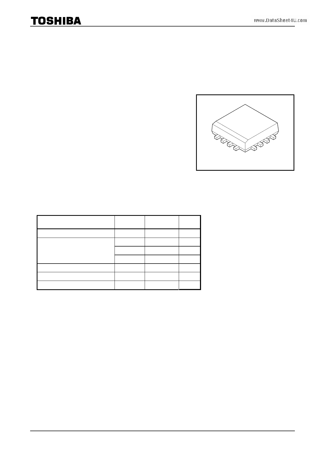
• Small package: QS16 (2.5 mm × 2.5 mm × 0.55 mm)
QS16
Weight: 0.0065 g (typ.)
Absolute Maximum Ratings (Ta = 25°C)
Characteristic
Symbol
Rating
Unit
Supply voltage
Input power
Power dissipation
www.DataShOepeetr4aUti.ncgomtemperature range
Storage temperature range
VCC (Note 1)
PIN (RF_IN)
PIN (LO_IN)
PIN (MIX_IN)
Pd (Note 2)
Topr
Tstg
4.5
10
0
0
500
−40 to +85
−55 to +150
V
dBmW
dBmW
dBmW
mW
°C
°C
Note:
Using continuously under heavy loads (e.g. the application of high temperature/current/voltage and the
significant change in temperature, etc.) may cause this product to decrease in the reliability significantly even
if the operating conditions (i.e. operating temperature/current/voltage, etc.) are within the absolute maximum
ratings and the operating ranges.
Please design the appropriate reliability upon reviewing the Toshiba Semiconductor Reliability Handbook
(“Handling Precautions”/“Derating Concept and Methods”) and individual reliability data (i.e. reliability test
report and estimated failure rate, etc).
Note 1: VCC = VCC1 = VCC2 = VCC3
Note 2: When mounted on a 30 mm × 35 mm × 0.6 mm FR4 substrate at Ta = 25°C (double-sided substrate: the
reverse side is ground connection)
Caution
This device is sensitive to electrostatic discharge. When handling this product, ensure that the environment is protected
against electrostatic discharge by using an earth strap, a conductive mat and an ionizer.
1 2007-11-01
1 page 
Typical Operating Characteristics of Low-Noise Amplifier Block
TA4500F
www.DataSheet4U.com
LNA Block
POUT(1-,2-tone),PIM3 vs PIN
VCC = 3 V, Ta = 25 °C,
RF1 = 1.9000 GHz,
RF2 = 1.9006 GHz for 2-tone, IM3 measurement
20
0
POUT (1-tone)
-20
POUT (2-tone)
-40
-60 PIM3
-80
-100
-50 -45 -40 -35 -30 -25 -20 -15 -10 -5
PIN (dBmW)
0
LNA Block
GLNA, IIP3LNA, NFLNA vs Temperature
VCC = 3 V,
RF1 = 1.9000 GHz/-35 dBmW,
RF2 = 1.9006 GHz/-35 dBmW for IIP3 measurement
16.8 3
16.6
16.4
GLNA
2.75
2.5
16.2 2.25
16.0
15.8
NFLNA
2
1.75
15.6 1.5 -7.2
15.4 1.25 -7.5
15.2
15.0
IIP3LNA
1 -7.8
0.75 -8.1
14.8 0.5 -8.4
14.6 0.25 -8.7
14.4
-60 -40 -20
0
0 -9.0
20 40 60 80 100
Ta (°C)
LNA Block
GLNA, IIP3LNA, NFLNA vs VCC
Ta = 25 °C,
RF1 = 1.9000 GHz/-35 dBmW,
RF2 = 1.9006 GHz/-35 dBmW for IIP3 measurement
16.60
16.55
16.50
GLNA
3
2.75
2.5
16.45
16.40
NFLNA
2.25
2
16.35
1.75
16.30
1.5 -7.3
16.25
IIP3LNA
1.25 -7.4
16.20
1 -7.5
16.15
0.75 -7.6
16.10
0.5 -7.7
16.05
0.25 -7.8
16.00
0 -7.9
2.0 2.5 3.0 3.5 4.0 4.5 5.0
VCC (V)
POUT(1-tone) [dBmW]
POUT(2-tone) [dBmW]
PIM3 [dBmW])
GLNA [dB]
NFLNA [dB]
IIP3LNA [dBmW])
GLNA [dB]
NFLNA [dB]
IIP3LNA [dBmW])
5 2007-11-01
5 Page 
Package Physical Dimensions
QS16
TA4500F
Unit: mm
www.DataSheet4U.com
Weight: 0.0065 g (typ.)
11
2007-11-01
11 Page | ||
| Páginas | Total 12 Páginas | |
| PDF Descargar | [ Datasheet TA4500F.PDF ] | |
Hoja de datos destacado
| Número de pieza | Descripción | Fabricantes |
| TA4500F | 1.9 GHz Band RX Front-End IC | Toshiba Semiconductor |
| Número de pieza | Descripción | Fabricantes |
| SLA6805M | High Voltage 3 phase Motor Driver IC. |
Sanken |
| SDC1742 | 12- and 14-Bit Hybrid Synchro / Resolver-to-Digital Converters. |
Analog Devices |
|
DataSheet.es es una pagina web que funciona como un repositorio de manuales o hoja de datos de muchos de los productos más populares, |
| DataSheet.es | 2020 | Privacy Policy | Contacto | Buscar |