|
|
|
PDF FAN103 Data sheet ( Hoja de datos )
| Número de pieza | FAN103 | |
| Descripción | Primary-Side-Regulation PWM Controller | |
| Fabricantes | Fairchild Semiconductor | |
| Logotipo | ||
Hay una vista previa y un enlace de descarga de FAN103 (archivo pdf) en la parte inferior de esta página. Total 16 Páginas | ||
|
No Preview Available !
October 2009
FAN103
Primary-Side-Regulation PWM Controller
Features
Low Standby Power Under 30mW
High Voltage Startup
Fewest External Component Counts
Constant-Voltage (CV) and Constant-Current (CC)
Control without Secondary-Feedback Circuitry
Green-Mode Function: Linearly-Decreasing PWM
Frequency
Fixed PWM Frequency at 50kHz with Frequency
Hopping to Solve EMI Problem
Cable Compensation in CV Mode
Peak-Current-Mode Control in CV Mode
Cycle-by-Cycle Current Limiting
VDD Over-Voltage Protection with Auto Restart
VDD Under-Voltage Lockout (UVLO)
Gate Output Maximum Voltage Clamped at 15V
Fixed Over-Temperature Protection with
Auto Restart
Available in the 8-Lead SOP Package
www.DataSheet4U.com
Applications
Battery chargers for cellular phones, cordless
phones, PDA, digital cameras, power tools, etc.
Replaces linear transformer and RCC SMPS
Description
This third-generation Primary-Side-Regulation (PSR)
and highly integrated PWM controller provides several
features to enhance the performance of low-power
flyback converters. The proprietary topology,
TURECURRENT™, of FAN103 enables precise CC
regulation and simplified circuit for battery charger
applications. A low-cost, smaller and lighter charger
results as compared to a conventional design or a linear
transformer.
To minimize standby power consumption, the
proprietary green-mode function provides off-time
modulation to linearly decrease PWM frequency under
light-load conditions. This green mode assists the power
supply in meeting the power conservation requirement.
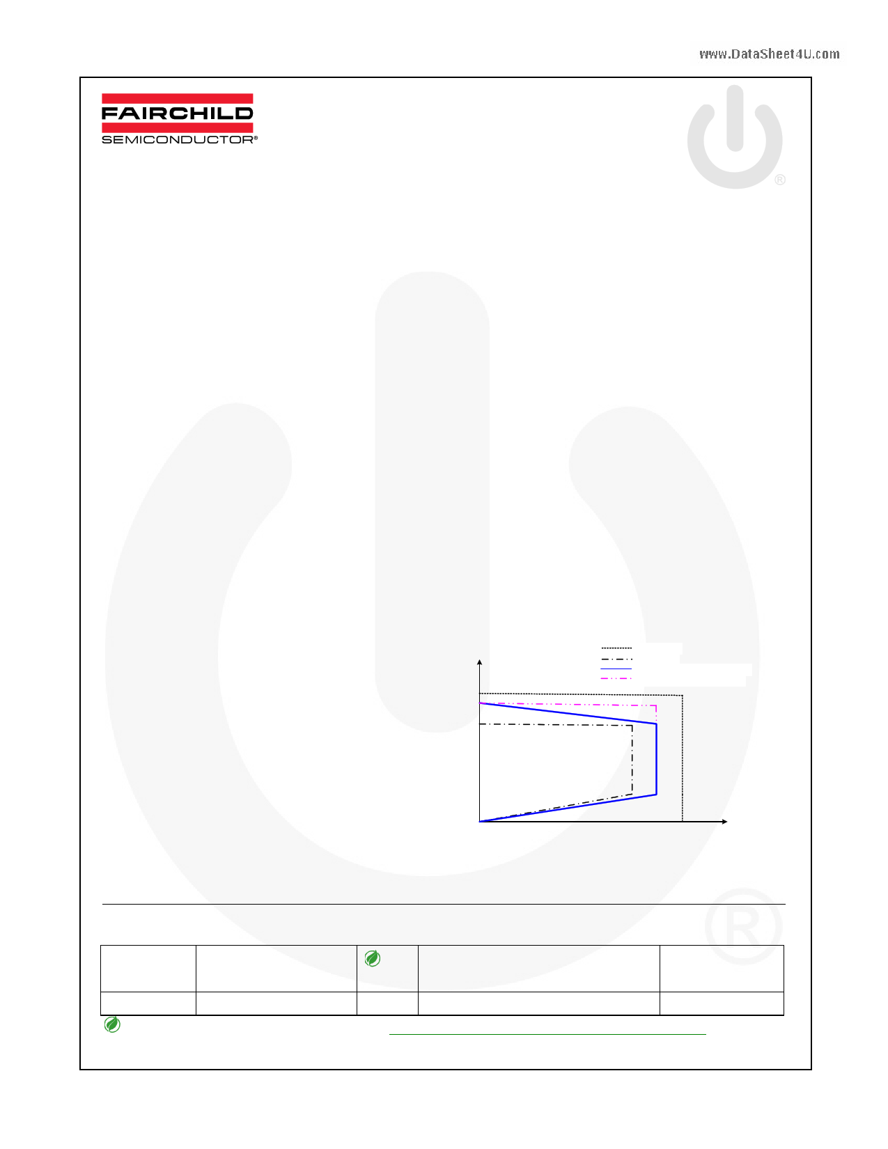
By using the FAN103, a charger can be implemented
with few external components and minimized cost. A
typical output CV/CC characteristic envelope is shown
in Figure 1.
VO
Maximum
Minimum
Before Cable Compensation
After Cable Compensation
IO
Figure 1. Typical Output V-I Characteristic
Ordering Information
Part Number
FAN103MY
Operating
Temperature Range
-40°C to +105°C
Eco
Status
Package
Packing Method
Green 8-Lead, Small Outline Package (SOP-8) Tape & Reel
For Fairchild’s definition of Eco Status, please visit: http://www.fairchildsemi.com/company/green/rohs_green.html
© 2009 Fairchild Semiconductor Corporation
FAN103 • Rev. 1.0.1
www.fairchildsemi.com
1 page 
Electrical Characteristics
Unless otherwise specified, VDD=15V and TA=25°C.
Symbol
Parameter
Conditions
VDD Section
VOP Continuously Operating Voltage
VDD-ON Turn-On Threshold Voltage
VDD-OFF Turn-Off Threshold Voltage
IDD-OP Operating Current
IDD-GREEN Green-Mode Operating Supply Current
VDD-OVP VDD Over-Voltage Protection Level
VDD-OVP- Hysteresis Voltage for VDD OVP
HYST
tD-VDDOVP VDD Over-Voltage-Protection Debounce Time
HV Startup Current Source Section
VHV-MIN Minimum Startup Voltage on HV Pin
IHV
IHV-LC
Supply Current Drawn from Pin HV
Leakage Current after Startup
VDC=100V
HV=500V, VDD=VDD-
OFF +1V
Oscillator Section
Center Frequency
fOSC
Frequency
Frequency Hopping Range
tFHR
fOSC-N-MIN
fOSC-CM-MIN
fDV
fDT
Frequency Hopping Period
Minimum Frequency at No-Load
Minimum Frequency at CCM
Frequency Variation vs. VDD Deviation
Frequency Variation vs. Temperature
Deviation
VDD=10~25V
TA=-40°C to +105°C
www.DataShVeoeltt4aUg.ceo-mError-Amplifier Section
VVR Reference Voltage
VN Green-Mode Starting Voltage on EA_V
VG Green-Mode Ending Voltage on EA_V
fOSC=-2kHz
fOSC=1kHz
Voltage-Sense Section
VBIAS-COMV Adaptive Bias Voltage Dominated by VCOMV
Itc IC Bias Current
Current-Sense Section
tPD Propagation Delay to GATE Output
tMIN-N Minimum On Time at No-Load
VTH Threshold Voltage for Current Limit
VTL
Threshold Voltage on VS Pin Smaller than
0.5V
RVS=20kΩ
VCOMR=1V
Min.
15
4.5
1.5
90
47
±1.5
2.475
Typ.
16
5.0
3.2
0.95
28
2.0
200
1.2
0.5
50
±2.0
3
370
13
1
2.500
2.5
0.5
1.4
10
90
950
0.8
0.25
Max.
25
17
5.5
5.0
1.20
2.5
350
50
3.0
3.0
53
±2.5
2
15
2.525
200
Units
V
V
V
mA
mA
V
V
µs
V
mA
µA
kHz
ms
Hz
kHz
%
%
V
V
V
V
µA
ns
ns
V
V
Continued on the following page…
© 2009 Fairchild Semiconductor Corporation
FAN103 • Rev. 1.0.1
5
www.fairchildsemi.com
5 Page 
Cable Voltage Drop Compensation
When it comes to cellular phone charger applications,
the battery is located at the end of cable, which causes,
typically, several percentage of voltage drop on the
actual battery voltage. FAN103 has a built-in cable
voltage drop compensation, which provides a constant
output voltage at the end of the cable over the entire
load range in CV mode. As load increases, the voltage
drop across the cable is compensated by increasing the
reference voltage of voltage regulation error amplifier.
Operating Current
The operating current in FAN103 is as small as 3.2mA.
The small operating current results in higher efficiency
and reduces the VDD hold-up capacitance requirement.
Once FAN103 enters deep-green mode, the operating
current is reduced to 0.95mA, assisting the power
supply in meeting power conservation requirements.
Green-Mode Operation
The FAN103 uses voltage regulation error amplifier
output (VCOMV) as an indicator of the output load and
modulates the PWM frequency, as shown in Figure 23.
The switching frequency decreases as load decreases.
In heavy load conditions, the switching frequency is
fixed at 50kHz. Once VCOMV decreases below 2.5V, the
PWM frequency linearly decreases from 50kHz. When
FAN103 enters into deep-green mode, the PWM
frequency is reduced to a minimum frequency of 370Hz,
gaining power saving to help meet international power
conservation requirements.
www.DataSheet4U.com
Figure 24. Frequency Hopping
High-Voltage Startup
Figure 25 shows the HV-startup circuit for FAN103
applications. The HV pin is connected to the line input or
bulk capacitor through a resistor, RSTART (100kΩ is
recommended). During startup, the internal startup
circuit in FAN103 is enabled. Meanwhile, line input
supplies the current, ISTARTUP, to charge the hold-up
capacitor, CDD, through RSTART. When the VDD voltage
reaches VDD-ON, the internal startup circuit is disabled,
blocking ISTARTUP from flowing into the HV pin. Once the
IC turns on, CDD is the only energy source to supply the
IC consumption current before the PWM starts to
switch. Thus, CDD must be large enough to prevent VDD
from dropping to VDD-OFF before the power can be
delivered from the auxiliary winding.
Figure 23. Switching Frequency in Green Mode
Frequency Hopping
EMI reduction is accomplished by frequency hopping,
which spreads the energy over a wider frequency range
than the bandwidth measured by the EMI test
equipment. FAN103 has an internal frequency hopping
circuit that changes the switching frequency between
47kHz and 53kHz with a period, as shown in Figure 24.
© 2009 Fairchild Semiconductor Corporation
FAN103 • Rev. 1.0.1
11
Figure 25. HV Startup Circuit
www.fairchildsemi.com
11 Page | ||
| Páginas | Total 16 Páginas | |
| PDF Descargar | [ Datasheet FAN103.PDF ] | |
Hoja de datos destacado
| Número de pieza | Descripción | Fabricantes |
| FAN100 | Primary-Side-Control PWM Controller | Fairchild Semiconductor |
| FAN102 | Primary-Side-Control PWM Controller | Fairchild Semiconductor |
| FAN103 | Primary-Side-Regulation PWM Controller | Fairchild Semiconductor |
| FAN104 | Case Fan 120x120 | LogiLink |
| Número de pieza | Descripción | Fabricantes |
| SLA6805M | High Voltage 3 phase Motor Driver IC. |
Sanken |
| SDC1742 | 12- and 14-Bit Hybrid Synchro / Resolver-to-Digital Converters. |
Analog Devices |
|
DataSheet.es es una pagina web que funciona como un repositorio de manuales o hoja de datos de muchos de los productos más populares, |
| DataSheet.es | 2020 | Privacy Policy | Contacto | Buscar |