|
|
|
PDF MAX1275 Data sheet ( Hoja de datos )
| Número de pieza | MAX1275 | |
| Descripción | (MAX1274 / MAX1275) 12-Bit ADCs | |
| Fabricantes | Maxim Integrated Products | |
| Logotipo | ||
Hay una vista previa y un enlace de descarga de MAX1275 (archivo pdf) en la parte inferior de esta página. Total 18 Páginas | ||
|
No Preview Available !
19-3158; Rev 0; 1/04
www.DataSheet4U.com
1.8Msps, Single-Supply, Low-Power,
True-Differential, 12-Bit ADCs
General Description
The MAX1274/MAX1275 low-power, high-speed, serial-
output, 12-bit, analog-to-digital converters (ADCs) oper-
ate at up to 1.8Msps. These devices feature true-differen-
tial inputs, offering better noise immunity, distortion
improvements, and a wider dynamic range over single-
ended inputs. A standard SPI™/QSPI™/MICROWIRE™
interface provides the clock necessary for conversion.
These devices easily interface with standard digital signal
processor (DSP) synchronous serial interfaces.
The MAX1274/MAX1275 operate from a single +4.75V to
+5.25V supply voltage and require an external reference.
The MAX1274 has a unipolar analog input, while the
MAX1275 has a bipolar analog input. These devices fea-
ture a partial power-down mode and a full power-down
mode for use between conversions, which lower the sup-
ply current to 1mA (typ) and 1µA (max), respectively. Also
featured is a separate power-supply input (VL), which
allows direct interfacing to +1.8V to VDD digital logic. The
fast conversion speed, low-power dissipation, excellent
AC performance, and DC accuracy (±1 LSB INL) make
the MAX1274/MAX1275 ideal for industrial process con-
trol, motor control, and base-station applications.
The MAX1274/MAX1275 come in a 12-pin TQFN pack-
age, and are available in the commercial (0°C to +70°C)
and extended (-40°C to +85°C) temperature ranges.
Data Acquisition
Bill Validation
Motor Control
Applications
Communications
Portable Instruments
Pin Configuration
Features
♦ 1.8Msps Sampling Rate
♦ Only 45mW (typ) Power Dissipation
♦ Only 1µA (max) Shutdown Current
♦ High-Speed, SPI-Compatible, 3-Wire Serial Interface
♦ 70dB S/(N + D) at 525kHz Input Frequency
♦ Internal True-Differential Track/Hold (T/H)
♦ External Reference
♦ No Pipeline Delays
♦ Small 12-Pin TQFN Package
Ordering Information
PART
TEMP RANGE
PIN-
PACKAGE
MAX1274ACTC-T
MAX1274BCTC-T
MAX1274AETC-T
MAX1274BETC-T
MAX1275ACTC-T
MAX1275BCTC-T
MAX1275AETC-T
MAX1275BETC-T
0°C to +70°C
0°C to +70°C
-40°C to +85°C
-40°C to +85°C
0°C to +70°C
0°C to +70°C
-40°C to +85°C
-40°C to +85°C
12 TQFN-12
12 TQFN-12
12 TQFN-12
12 TQFN-12
12 TQFN-12
12 TQFN-12
12 TQFN-12
12 TQFN-12
INPUT
Unipolar
Unipolar
Unipolar
Unipolar
Bipolar
Bipolar
Bipolar
Bipolar
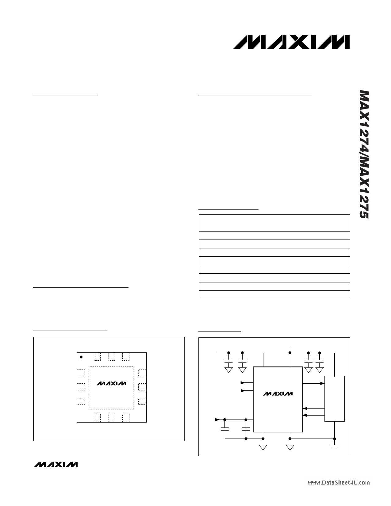
Typical Operating Circuit
TOP VIEW
AIN+ N.C. SCLK
12 11 10
AIN- 1
REF 2
RGND 3
MAX1274
MAX1275
9 CNVST
8 DOUT
7 VL
456
VDD N.C. GND
TQFN
4.75V TO +5.25V
+1.8V TO VDD
10µF
DIFFERENTIAL +
INPUT
VOLTAGE -
REF
4.7µF
0.01µF
0.01µF
VDD
0.01µF
VL
AIN+ DOUT
AIN-
MAX1274
MAX1275 CNVST
SCLK
REF
RGND
GND
10µF
µC/DSP
SPI/QSPI are trademarks of Motorola, Inc.
MICROWIRE is a trademark of National Semiconductor Corp.
________________________________________________________________ Maxim Integrated Products 1
For pricing, delivery, and ordering information, please contact Maxim/Dallas Direct! at
1-888-629-4642, or visit Maxim’s website at www.maxim-ic.com.
1 page 
www.DataSheet4U.com
1.8Msps, Single-Supply, Low-Power,
True-Differential, 12-Bit ADCs
Typical Operating Characteristics
(VDD = +5V, VL = VDD, VREF = 4.096V, fSCLK = 28.8MHz, TA = TMIN to TMAX, unless otherwise noted. Typical values are measured
at TA = +25°C)
INTEGRAL NONLINEARITY
vs. DIGITAL OUTPUT CODE (MAX1274)
0.8
INTEGRAL NONLINEARITY
vs. DIGITAL OUTPUT CODE (MAX1275)
0.8
DIFFERENTIAL NONLINEARITY
vs. DIGITAL OUTPUT CODE (MAX1274)
0.8
0.6 0.6 0.6
0.4 0.4 0.4
0.2 0.2 0.2
0 00
-0.2 -0.2 -0.2
-0.4 -0.4 -0.4
-0.6 -0.6 -0.6
-0.8
0
1000 2000 3000 4000 5000
DIGITAL OUTPUT CODE
-0.8
0
1000 2000 3000 4000
DIGITAL OUTPUT CODE
5000
-0.8
0
1000 2000 3000 4000
DIGITAL OUTPUT CODE
5000
DIFFERENTIAL NONLINEARITY
vs. DIGITAL OUTPUT CODE (MAX1275)
0.8
0.6
0.4
0.2
0
-0.2
-0.4
-0.6
-0.8
0
1000 2000 3000 4000 5000
DIGITAL OUTPUT CODE
OFFSET ERROR
vs. TEMPERATURE (MAX1274)
0.4
0.3
0.2
0.1
0
-0.1
-0.2
-0.3
-0.4
-40
-15 10 35 60
TEMPERATURE (°C)
85
OFFSET ERROR
vs. TEMPERATURE (MAX1275)
1.00
0.75
0.50
0.25
0
-0.25
-0.50
-0.75
-1.00
-40
-15 10 35 60
TEMPERATURE (°C)
85
GAIN ERROR
vs. TEMPERATURE (MAX1274)
-0.5
-1.0
-1.5
GAIN ERROR
vs. TEMPERATURE (MAX1275)
-0.5
-1.0
-1.5
FFT PLOT (MAX1274)
0
fSAMPLE = 2Msps
-20 fSCLK = 32MHz
fIN = 100kHz
-40
SINAD = 70.74dB
SNR = 70.82dB
THD = -88.63dB
-60 SFDR = 87.07dB
-2.0 -2.0 -80
-100
-2.5 -2.5
-120
-3.0
-40
-15 10 35 60
TEMPERATURE (°C)
85
-3.0
-40
-15 10 35 60
TEMPERATURE (°C)
85
-140
0
200 400 600 800
ANALOG INPUT FREQUENCY (kHz)
1000
_______________________________________________________________________________________ 5
5 Page 
www.DataSheet4U.com
1.8Msps, Single-Supply, Low-Power,
True-Differential, 12-Bit ADCs
Partial Power-Down and
Full Power-Down Modes
Power consumption can be reduced significantly by plac-
ing the MAX1274/MAX1275 in either partial power-down
mode or full power-down mode. Partial power-down
mode is ideal for infrequent data sampling and fast wake-
up time applications. Pull CNVST high after the 3rd SCLK
rising edge and before the 14th SCLK rising edge to
enter and stay in partial power-down mode (see Figure
6). This reduces the supply current to 1mA. Drive CNVST
low and allow at least 14 SCLK cycles to elapse before
driving CNVST high to exit partial power-down mode.
Full power-down mode is ideal for infrequent data sam-
pling and very low supply current applications. The
MAX1274/MAX1275 have to be in partial power-down
mode in order to enter full power-down mode. Perform
the SCLK/CNVST sequence described above to enter
partial power-down mode. Then repeat the same
sequence to enter full power-down mode (see Figure
7). Drive CNVST low, and allow at least 14 SCLK cycles
to elapse before driving CNVST high to exit full power-
down mode. In partial/full power-down mode, maintain
a logic low or a logic high on SCLK to minimize power
consumption.
Transfer Function
Figure 8 shows the unipolar transfer function for the
MAX1274. Figure 9 shows the bipolar transfer function for
the MAX1275. The MAX1274 output is straight binary,
while the MAX1275 output is two’s complement.
Applications Information
External Reference
An external reference is required for the MAX1274/
MAX1275. Use a 4.7µF and 0.01µF bypass capacitor on
the REF pin for best performance. The reference input
structure allows a voltage range of +1V to VDD.
How to Start a Conversion
An analog-to-digital conversion is initiated by CNVST,
clocked by SCLK, and the resulting data is clocked out
on DOUT by SCLK. With SCLK idling high or low, a falling
edge on CNVST begins a conversion. This causes the
analog input stage to transition from track to hold mode,
and for DOUT to transition from high impedance to being
actively driven low. A total of 16 SCLK cycles are required
to complete a normal conversion. If CNVST is low during
the 16th falling SCLK edge, DOUT returns to high imped-
ance on the next rising edge of CNVST or SCLK,
enabling the serial interface to be shared by multiple
devices. If CNVST returns high after the 14th, but before
the 16th SCLK rising edge, DOUT remains active so con-
tinuous conversions can be sustained. The highest
throughput is achieved when performing continuous con-
versions. Figure 10 illustrates a conversion using a typical
serial interface.
CNVST
SCLK
DOUT
MODE
FIRST 8-BIT TRANSFER
EXECUTE PARTIAL POWER-DOWN TWICE
SECOND 8-BIT TRANSFER
1ST SCLK RISING EDGE
1ST SCLK RISING EDGE
0 0 0 D11 D10 D9 D8 D7
DOUT ENTERS TRI-STATE ONCE CNVST GOES HIGH
00000000
NORMAL
PPD RECOVERY FPD
Figure 7. SPI Interface—Full Power-Down Mode
______________________________________________________________________________________ 11
11 Page | ||
| Páginas | Total 18 Páginas | |
| PDF Descargar | [ Datasheet MAX1275.PDF ] | |
Hoja de datos destacado
| Número de pieza | Descripción | Fabricantes |
| MAX127 | Multirange / +5V / 12-Bit DAS with 2-Wire Serial Interface | Maxim Integrated |
| MAX1270 | Serial 12-Bit ADCs | Maxim Integrated |
| MAX1271 | Serial 12-Bit ADCs | Maxim Integrated |
| MAX1272 | 12-Bit ADCs | Maxim Integrated |
| Número de pieza | Descripción | Fabricantes |
| SLA6805M | High Voltage 3 phase Motor Driver IC. |
Sanken |
| SDC1742 | 12- and 14-Bit Hybrid Synchro / Resolver-to-Digital Converters. |
Analog Devices |
|
DataSheet.es es una pagina web que funciona como un repositorio de manuales o hoja de datos de muchos de los productos más populares, |
| DataSheet.es | 2020 | Privacy Policy | Contacto | Buscar |