|
|
|
PDF ICS5314I-11 Data sheet ( Hoja de datos )
| Número de pieza | ICS5314I-11 | |
| Descripción | DIFFERENTIAL-TO-2.5V/3.3V LVPECL FANOUT BUFFER | |
| Fabricantes | Integrated Circuit Systems | |
| Logotipo | ||
Hay una vista previa y un enlace de descarga de ICS5314I-11 (archivo pdf) en la parte inferior de esta página. Total 18 Páginas | ||
|
No Preview Available !
www.DataSheet4U.com Integrated
Circuit
Systems, Inc.
ICS85314I-11
LOW SKEW, 1-TO-5
DIFFERENTIAL-TO-2.5V/3.3V LVPECL FANOUT BUFFER
GENERAL DESCRIPTION
FEATURES
The ICS85314I-11 is a low skew, high perfor- • 5 differential 2.5V/3.3V LVPECL outputs
ICS
HiPerClockS™
mance 1-to-5 Differential-to-2.5V/3.3V LVPECL
fanout buffer and a member of the HiPerClockS™
• Selectable differential CLKx, nCLKx inputs
family of High Performance Clock Solutions from • CLK0, nCLK0 and CLK1, nCLK1 pairs can accept the
ICS. The ICS85314I-11 has two selectable dif- following differential input levels: LVPECL, LVDS, LVHSTL,
ferential clock inputs. The CLK0, nCLK0 and CLK1, nCLK1 HCSL, SSTL
pairs can accept most standard differential input levels. The
clock enable is internally synchronized to eliminate runt clock • Maximum output frequency: 700MHz
pulses on the outputs during asynchronous assertion/ • Translates any single-ended input signal to 3.3V
deassertion of the clock enable pin.
LVPECL levels with resistor bias on nCLK input
Guaranteed output and part-to-part skew characteristics make
the ICS85314I-11 ideal for those applications demanding well
defined performance and repeatability.
• Output skew: 30ps (maximum)
• Part-to-part skew: 350ps (maximum)
• Propagation delay: 1.8ns (maximum)
• RMS phase jitter @ 155.52MHz (12kHz - 20MHz):
0.05ps (typical)
• LVPECL mode operating voltage supply range:
V = 2.375V to 3.8V, V = 0V
CC EE
• -40°C to 85°C ambient operating temperature
• Available in both standard and lead-free RoHS-compliant
packages
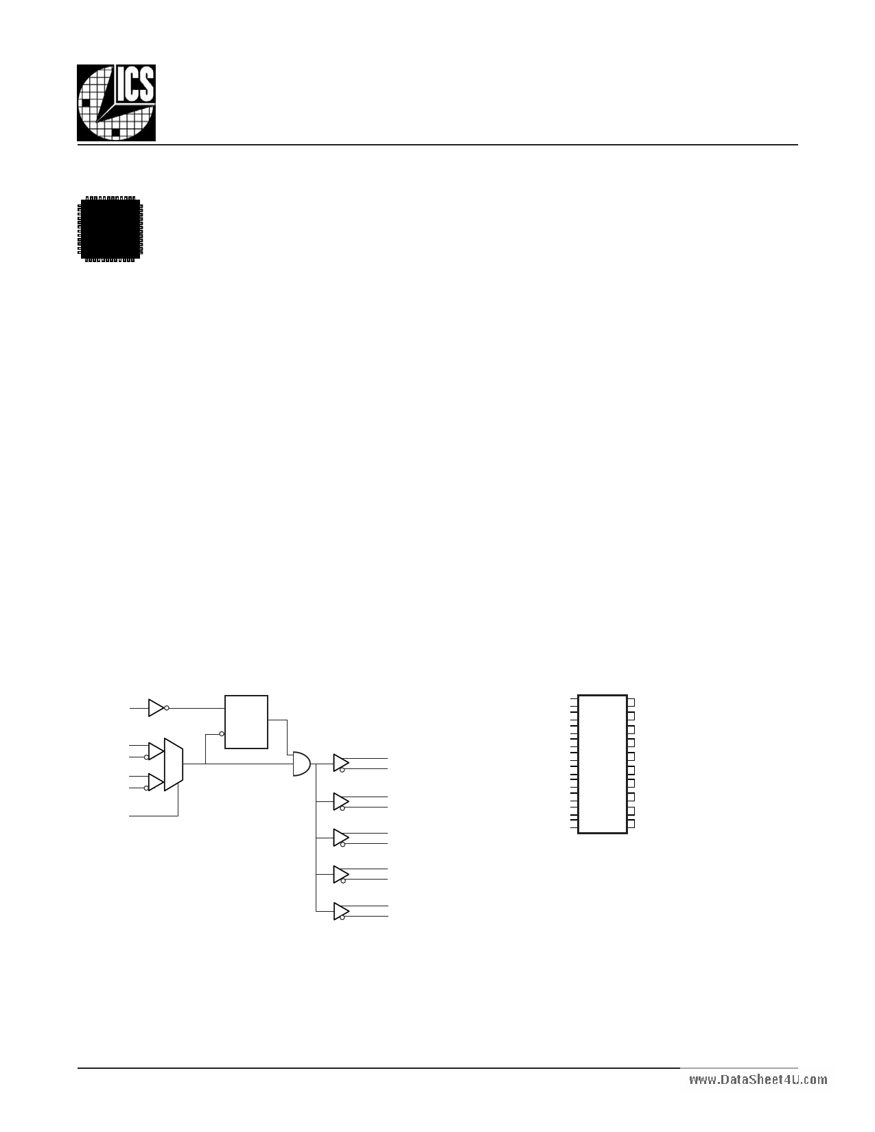
BLOCK DIAGRAM
nCLK_EN
CLK0
nCLK0
CLK1
nCLK1
CLK_SEL
00
11
D
Q
CK
PIN ASSIGNMENT
Q0 1
20 VCC
nQ0 2
19 nCLK_EN
Q1 3
18 VCC
nQ1 4
17 nCLK1
Q0
Q2 5
16 CLK1
nQ0
nQ2 6
15 RESERVED
Q1
nQ1
Q3 7
nQ3 8
Q4 9
14 nCLK0
13 CLK0
12 CLK_SEL
Q2 nQ4 10 11 VEE
nQ2
ICS85314I-11
Q3 20-Lead TSSOP
nQ3 6.5mm x 4.4mm x 0.92mm Package Body
Q4
nQ4
G Package
Top View
ICS85314I-11
20-Lead SOIC
7.5mm x 12.8mm x 2.3mm Package Body
M Package
Top View
85314AGI-11
www.icst.com/products/hiperclocks.html
1
REV. C MAY 24, 2005
1 page 
www.DataSheet4U.com Integrated
Circuit
Systems, Inc.
ICS85314I-11
LOW SKEW, 1-TO-5
DIFFERENTIAL-TO-2.5V/3.3V LVPECL FANOUT BUFFER
TABLE 4D. LVPECL DC CHARACTERISTICS, VCC = 2.375V TO 3.8V, VEE = 0V, TA = -40°C TO 85°C
Symbol Parameter
Test Conditions
Minimum Typical
VOH Output High Voltage; NOTE 1
VOL Output Low Voltage; NOTE 1
VSWING Peak-to-Peak Output Voltage Swing
NOTE 1: Outputs terminated with 50Ω to VCC - 2V.
VCC - 1.4
VCC - 2.0
0.6
Maximum
VCC - 0.9
VCC - 1.7
1.0
Units
V
V
V
TABLE
5.
AC
CHARACTERISTICS,
V
CC
=
2.375V
TO
3.8V,
V
EE
=
0V,
TA
=
-40°C
TO
85°C
Symbol Parameter
Test Conditions
Minimum Typical Maximum
fMAX
tp
LH
tsk(o)
tjit (Ø)
tsk(pp)
Output Frequency
Propagation Delay, Low to High;
NOTE 1
Output Skew; NOTE 2, 5
RMS Phase Jitter (Random);
NOTE 4
Part-to-Part Skew; NOTE 3, 5
IJ 700MHz
Integration Range:
(12kHz - 20MHz)
700
1.0 1.4 1.8
30
0.05
350
tS
tH
tR / tF
odc
Setup Time
Hold Time
Output Rise/Fall Time
Output Duty Cycle
nCLK_EN to CLK
nCLK_EN to CLK
20% to 80%
IJ 700MHz
50
50
200
45
All parameters measured at fMAX unless noted otherwise.
The cycle-to-cycle jitter on the input will equal the jitter on the output. The part does not add jitter
NOTE 1: Measured from the differential input crossing point to the differential output crossing point.
NOTE 2: Defined as skew between outputs at the same supply voltage and with equal load conditions.
Measured at the output differential cross points.
NOTE 3: Defined as skew between outputs on different devices operating at the same supply voltages
and with equal load conditions. Using the same type of inputs on each device, the outputs are measured
at the differential cross points.
NOTE 4: Please refer to Phase Noise Plot.
NOTE 5: This parameter is defined in accordance with JEDEC Standard 65.
700
55
Units
MHz
ns
ps
ps
ps
ps
ps
ps
ps
85314AGI-11
www.icst.com/products/hiperclocks.html
5
REV. C MAY 24, 2005
5 Page 
www.DataSheet4U.com Integrated
Circuit
Systems, Inc.
ICS85314I-11
LOW SKEW, 1-TO-5
DIFFERENTIAL-TO-2.5V/3.3V LVPECL FANOUT BUFFER
TERMINATION FOR 2.5V LVPECL OUTPUT
Figure 5A and Figure 5B show examples of termination for
2.5V LVPECL driver. These terminations are equivalent to ter-
minating 50Ω to VCC - 2V. For VCC = 2.5V, the VCC - 2V is very
close to ground level. The R3 in Figure 5B can be eliminated
and the termination is shown in Figure 5C.
VCC=2.5V
Zo = 50 Ohm
Zo = 50 Ohm
2,5V LVPECL
Driv er
2.5V
R1 R3
250 250
2.5V
+
-
R2
62.5
R4
62.5
FIGURE 5A. 2.5V LVPECL DRIVER TERMINATION EXAMPLE
VCC=2.5V
Zo = 50 Ohm
Zo = 50 Ohm
2,5V LVPECL
Driv er
2.5V
+
-
R1 R2
50 50
R3
18
FIGURE 5B. 2.5V LVPECL DRIVER TERMINATION EXAMPLE
VCC=2.5V
Zo = 50 Ohm
Zo = 50 Ohm
2,5V LVPECL
Driv er
2.5V
+
-
R1 R2
50 50
FIGURE 5C. 2.5V LVPECL TERMINATION EXAMPLE
85314AGI-11
www.icst.com/products/hiperclocks.html
11
REV. C MAY 24, 2005
11 Page | ||
| Páginas | Total 18 Páginas | |
| PDF Descargar | [ Datasheet ICS5314I-11.PDF ] | |
Hoja de datos destacado
| Número de pieza | Descripción | Fabricantes |
| ICS5314I-11 | DIFFERENTIAL-TO-2.5V/3.3V LVPECL FANOUT BUFFER | Integrated Circuit Systems |
| Número de pieza | Descripción | Fabricantes |
| SLA6805M | High Voltage 3 phase Motor Driver IC. |
Sanken |
| SDC1742 | 12- and 14-Bit Hybrid Synchro / Resolver-to-Digital Converters. |
Analog Devices |
|
DataSheet.es es una pagina web que funciona como un repositorio de manuales o hoja de datos de muchos de los productos más populares, |
| DataSheet.es | 2020 | Privacy Policy | Contacto | Buscar |