|
|
|
PDF ICS5310I-01 Data sheet ( Hoja de datos )
| Número de pieza | ICS5310I-01 | |
| Descripción | ECL/LVPECL FANOUT BUFFER | |
| Fabricantes | Integrated Circuit Systems | |
| Logotipo | ||
Hay una vista previa y un enlace de descarga de ICS5310I-01 (archivo pdf) en la parte inferior de esta página. Total 15 Páginas | ||
|
No Preview Available !
www.DataSheet4U.com Integrated
Circuit
Systems, Inc.
ICS85310I-01
LOW SKEW, 1-TO-10
DIFFERENTIAL-TO-2.5V/3.3V ECL/LVPECL FANOUT BUFFER
GENERAL DESCRIPTION
The ICS85310I-01 is a low skew, high perfor-
ICS mance 1-to-10 Differential-to-2.5V/3.3V ECL/
HiPerClockS™ LVPECL Fanout Buffer and a member of the
HiPerClockS™ family of High Perfor mance
Clock Solutions from ICS. The CLKx, nCLKx
pairs can accept most standard differential input levels. The
ICS85310I-01 is characterized to operate from either a
2.5V or a 3.3V power supply. Guaranteed output and part-
to-part skew characteristics make the ICS85310I-01 ideal
for those clock distribution applications demanding well
defined performance and repeatability.
FEATURES
• Ten differential 2.5V/3.3V LVPECL / ECL outputs
• Two selectable differential input pairs
• CLKx, nCLKx pairs can accept the following differential
input levels: LVPECL, LVDS, LVHSTL, SSTL, HCSL
• Maximum output frequency: 700MHz
• Translates any single ended input signal to
3.3V LVPECL levels with resistor bias on nCLK input
• Output skew: 30ps (typical)
• Part-to-part skew: 140ps (typical)
• Propagation delay: 2ns (typical)
• Additive phase jitter, RMS: <0.13ps (typical)
• LVPECL mode operating voltage supply range:
V = 2.375V to 3.8V, V = 0V
CC EE
• ECL mode operating voltage supply range:
VCC = 0V, VEE = -2.375V to -3.8V
• -40°C to 85°C ambient operating temperature
• Available in both standard and lead-free RoHS compliant
packages
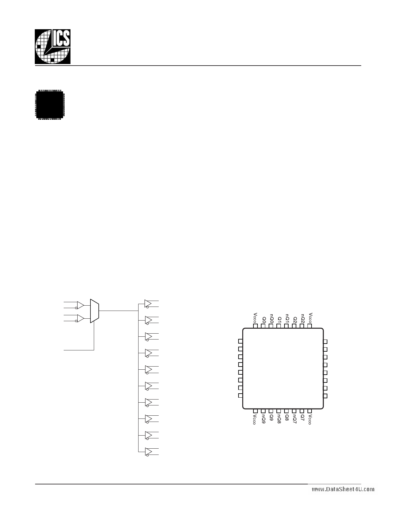
BLOCK DIAGRAM
CLK0
nCLK0
CLK1
nCLK1
0
1
CLK_SEL
PIN ASSIGNMENT
Q0
nQ0
Q1
nQ1
Q2
nQ2
32 31 30 29 28 27 26 25
VCC 1
24 Q3
Q3
nQ3
CLK_SEL
CLK0
2
3
23 nQ3
22 Q4
Q4
nQ4
nCLK0 4 ICS85310I-01 21 nQ4
nc 5
20 Q5
Q5
nQ5
CLK1
nCLK1
6
7
19 nQ5
18 Q6
Q6
nQ6
VEE 8
17 nQ6
9 10 11 12 13 14 15 16
Q7
nQ7
Q8 32-Lead LQFP
nQ8 7mm x 7mm x 1.4mm package body
Q9
nQ9
Y Package
Top View
85310AYI-01
www.icst.com/products/hiperclocks.html
1
REV. F JANUARY16, 2006
1 page 
www.DataSheet4U.com Integrated
Circuit
Systems, Inc.
ICS85310I-01
LOW SKEW, 1-TO-10
DIFFERENTIAL-TO-2.5V/3.3V ECL/LVPECL FANOUT BUFFER
ADDITIVE PHASE JITTER
The spectral purity in a band at a specific offset from the funda-
mental compared to the power of the fundamental is called the
dBc Phase Noise. This value is normally expressed using a
Phase noise plot and is most often the specified plot in many
applications. Phase noise is defined as the ratio of the noise
power present in a 1Hz band at a specified offset from the fun-
damental frequency to the power value of the fundamental. This
ratio is expressed in decibels (dBm) or a ratio of the power in
the 1Hz band to the power in the fundamental. When the re-
quired offset is specified, the phase noise is called a dBc value,
which simply means dBm at a specified offset from the funda-
mental. By investigating jitter in the frequency domain, we get a
better understanding of its effects on the desired application over
the entire time record of the signal. It is mathematically possible
to calculate an expected bit error rate given a phase noise plot.
0
-10
Additive Phase Jitter, RMS
-20 @ 155.52MHz = <0.13ps typical
-30
-40
-50
-60
-70
-80
-90
-100
-110
-120
-130
-140
-150
-160
-170
-180
-190
100
1k
10k 100k 1M
10M 100M
OFFSET FROM CARRIER FREQUENCY (HZ)
As with most timing specifications, phase noise measurements
have issues. The primary issue relates to the limitations of the
equipment. Often the noise floor of the equipment is higher than
the noise floor of the device. This is illustrated above. The de-
vice meets the noise floor of what is shown, but can actually be
lower. The phase noise is dependant on the input source and
measurement equipment.
85310AYI-01
www.icst.com/products/hiperclocks.html
5
REV. F JANUARY16, 2006
5 Page 
www.DataSheet4U.com Integrated
Circuit
Systems, Inc.
ICS85310I-01
LOW SKEW, 1-TO-10
DIFFERENTIAL-TO-2.5V/3.3V ECL/LVPECL FANOUT BUFFER
3. Calculations and Equations.
LVPECL output driver circuit and termination are shown in Figure 4.
VCCO
Q1
VOUT
RL
50
VCCO - 2V
Figure 4. LVPECL Driver Circuit and Termination
To calculate worst case power dissipation into the load, use the following equations which assume a 50Ω load, and a termination
voltage of V - 2V.
CCO
• For logic high, V = V
=V
– 1.0V
OUT
OH_MAX
CCO_MAX
(V - V ) = 1.0V
CCO_MAX OH_MAX
• For logic low, V = V = V
– 1.7V
OUT
OL_MAX
CCO_MAX
(V - V ) = 1.7V
CCO_MAX OL_MAX
Pd_H is power dissipation when the output drives high.
Pd_L is the power dissipation when the output drives low.
Pd_H = [(V – (V
- 2V))/R ] * (V
- V ) = [(2V - (V
- V ))/R ] * (V
-V )=
OH_MAX
CCO_MAX
L CCO_MAX OH_MAX
CCO_MAX
OH_MAX
L
CCO _MAX OH_MAX
[(2V - 1V)/50Ω] * 1V = 20.0mW
Pd_L = [(V – (V
- 2V))/R ] * (V
- V ) = [(2V - (V
- V ))/R ] * (V
-V )=
OL_MAX
CCO_MAX
L CCO_MAX OL_MAX
CCO_MAX
OL_MAX
L
CCO_MAX OL_MAX
[(2V - 1.7V)/50Ω] * 1.7V = 10.2mW
Total Power Dissipation per output pair = Pd_H + Pd_L = 30.2mW
85310AYI-01
www.icst.com/products/hiperclocks.html
11
REV. F JANUARY16, 2006
11 Page | ||
| Páginas | Total 15 Páginas | |
| PDF Descargar | [ Datasheet ICS5310I-01.PDF ] | |
Hoja de datos destacado
| Número de pieza | Descripción | Fabricantes |
| ICS5310I-01 | ECL/LVPECL FANOUT BUFFER | Integrated Circuit Systems |
| Número de pieza | Descripción | Fabricantes |
| SLA6805M | High Voltage 3 phase Motor Driver IC. |
Sanken |
| SDC1742 | 12- and 14-Bit Hybrid Synchro / Resolver-to-Digital Converters. |
Analog Devices |
|
DataSheet.es es una pagina web que funciona como un repositorio de manuales o hoja de datos de muchos de los productos más populares, |
| DataSheet.es | 2020 | Privacy Policy | Contacto | Buscar |