|
|
PDF TC6215 Data sheet ( Hoja de datos )
| Número de pieza | TC6215 | |
| Descripción | Enhancement-Mode Dual MOSFET | |
| Fabricantes | Supertex | |
| Logotipo |  |
|
Hay una vista previa y un enlace de descarga de TC6215 (archivo pdf) en la parte inferior de esta página. Total 5 Páginas | ||
|
No Preview Available !
www.DataSheet4U.com
N- and P-Channel
Enhancement-Mode Dual MOSFET
TC6215
Features
► Back to back gate-source Zener diodes
► Guaranteed RDS(ON) at 4.0V gate drive
► Low threshold
► Low on-resistance
► Independent N- and P-channels
► Electrically isolated N- and P-channels
► Low input capacitance
► Fast switching speeds
► Free from secondary breakdowns
► Low input and output leakage
Applications
► High voltage pulsers
► Amplifiers
► Buffers
► Piezoelectric transducer drivers
► General purpose line drivers
► Logic level interfaces
General Description
The Supertex TC6215 consists of high voltage, low threshold N-channel
and P-channel MOSFETs in an 8-Lead SOIC (TG) package. Both
MOSFETs have integrated back to back gate-source Zener diode clamps
and guaranteed RDS(ON) ratings down to 4.0V gate drive allowing them to
be driven directly with standard 5.0V CMOS logic.
These low threshold enhancement-mode (normally-off) transistors utilize
an advanced vertical DMOS structure and Supertex’s well-proven silicon-
gate manufacturing process. This combination produces devices with the
power handling capabilities of bipolar transistors and with the high input
impedance and positive temperature coefficient inherent in MOS devices.
Characteristic of all MOS structures, these devices are free from thermal
runaway and thermally-induced secondary breakdown.
Supertex’s vertical DMOS FETs are ideally suited to a wide range of
switching and amplifying applications where very low threshold voltage,
high breakdown voltage, high input impedance, low input capacitance,
and fast switching speeds are desired.
Ordering Information
Device
Package Option
8-Lead SOIC
4.90x3.90mm body
1.75mm height (max)
1.27mm pitch
BVDSS/BVDGS
N-Channel P-Channel
(V) (V)
TC6215
TC6215TG-G
-G indicates package is RoHS compliant (‘Green’)
150
-150
RDS(ON) (Max)
N-Channel P-Channel
(Ω) (Ω)
4.0 7.0
Absolute Maximum Ratings
Parameter
Value
Drain-to-source voltage
Drain-to-gate voltage
Gate-to-source voltage
BVDSS
BVDGS
±20V
Operating and storage temperature -55°C to + 150°C
Soldering temperature*
300°C
Absolute Maximum Ratings are those values beyond which damage to the device
may occur. Functional operation under these conditions is not implied. Continuous
operation of the device at the absolute rating level may affect device reliability. All
voltages are referenced to device ground.
* Distance of 1.6mm from case for 10 seconds.
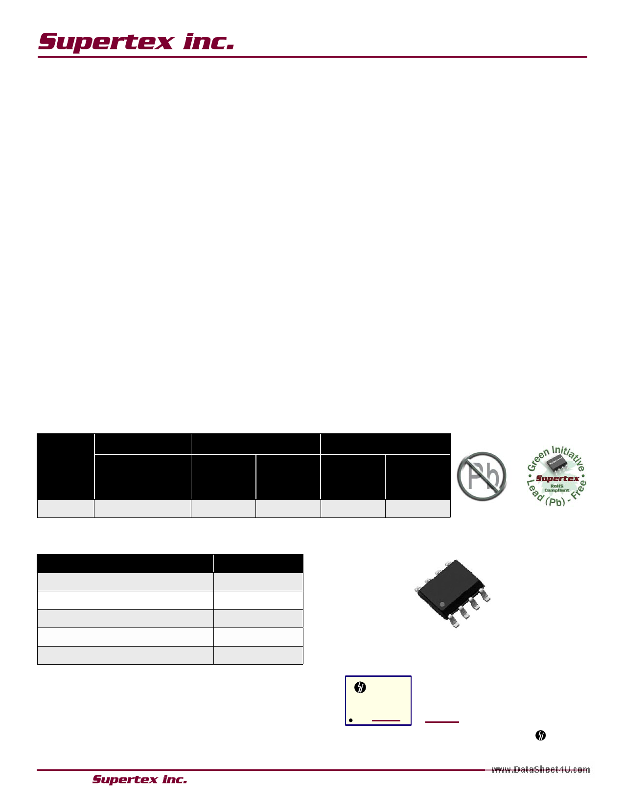
Pin Configuration
DP
DP
DN
DN
GP
SP
GN
SN
8-Lead SOIC (TG)
(top view)
Product Marking
YYWW
C6215
LLLL
YY = Year Sealed
WW = Week Sealed
L = Lot Number
= “Green” Packaging
Package may or may not include the following marks: Si or
8-Lead SOIC (TG)
● 1235 Bordeaux Drive, Sunnyvale, CA 94089 ● Tel: 408-222-8888 ● www.supertex.com
1 page 
TC6215
www.DataSheet4U.com
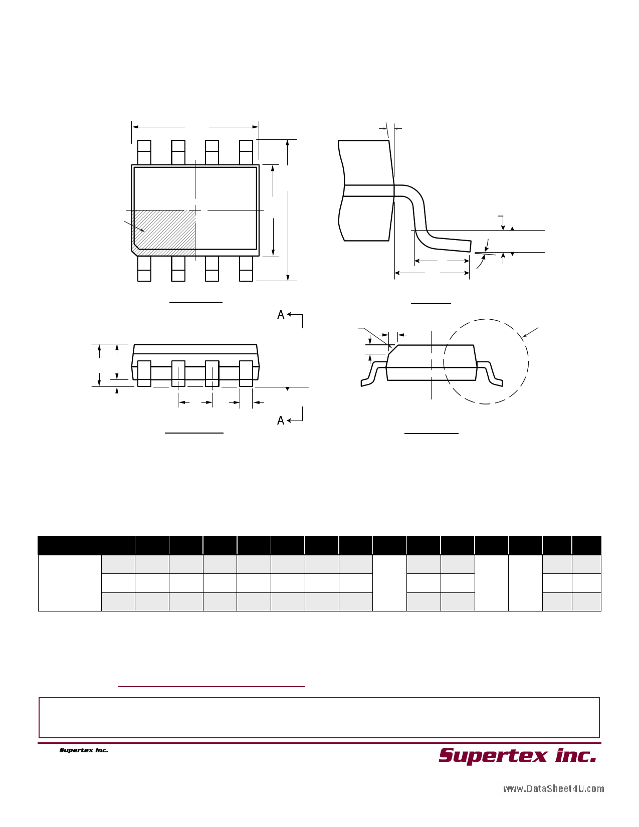
8-Lead SOIC (Narrow Body) Package Outline (TG)
4.90x3.90mm body, 1.75mm height (max), 1.27mm pitch
D
8
θ1
E
Note 1
(Index Area
D/2 x E1/2)
1
Top View
E1
A
A A2
A1
Seating
Plane
e
Side View
b
A
Note 1
h
L
L1
View B
h
L2 Gauge
Plane
Seating
θ Plane
View B
View A-A
Note:
1. This chamfer feature is optional. A Pin 1 identifier must be located in the index area indicated. The Pin 1 identifier can be: a molded mark/identifier;
an embedded metal marker; or a printed indicator.
Symbol
A A1 A2 b D E E1 e h L L1 L2 θ θ1
MIN 1.35* 0.10 1.25 0.31 4.80* 5.80* 3.80*
0.25 0.40
0O 5O
Dimension
(mm)
NOM
-
-
-
-
4.90
6.00
3.90
1.27
BSC
-
-
1.04 0.25
REF BSC
-
-
MAX 1.75 0.25 1.65* 0.51 5.00* 6.20* 4.00*
0.50 1.27
8O 15O
JEDEC Registration MS-012, Variation AA, Issue E, Sept. 2005.
* This dimension is not specified in the original JEDEC drawing. The value listed is for reference only.
Drawings are not to scale.
Supertex Doc. #: DSPD-8SOLGTG, Version H101708.
(The package drawing(s) in this data sheet may not reflect the most current specifications. For the latest package outline
information go to http://www.supertex.com/packaging.html.)
Supertex inc. does not recommend the use of its products in life support applications, and will not knowingly sell them for use in such applications unless it receives an
adequate “product liability indemnification insurance agreement.” Supertex inc. does not assume responsibility for use of devices described, and limits its liability to the
replacement of the devices determined defective due to workmanship. No responsibility is assumed for possible omissions and inaccuracies. Circuitry and specifications
are subject to change without notice. For the latest product specifications refer to the Supertex inc. website: http//www.supertex.com.
©2008
All rights reserved. Unauthorized use or reproduction is prohibited.
Doc.# DSFP-TC6215
A122208
1235 Bordeaux Drive, Sunnyvale, CA 94089
Tel: 408-222-8888
www.supertex.com
5
5 Page | ||
| Páginas | Total 5 Páginas | |
| PDF Descargar | [ Datasheet TC6215.PDF ] | |
Hoja de datos destacado
| Número de pieza | Descripción | Fabricantes |
| TC621 | (TC620 / TC621) Dual Trip Point Temperature Sensors | Microchip Technology |
| TC621 | (TC620 / TC621) DUAL TRIP POINT TEMPERATURE SENSORS | TelCom Semiconductor |
| TC6215 | Enhancement-Mode Dual MOSFET | Supertex |
| Número de pieza | Descripción | Fabricantes |
| SLA6805M | High Voltage 3 phase Motor Driver IC. |
Sanken |
| SDC1742 | 12- and 14-Bit Hybrid Synchro / Resolver-to-Digital Converters. |
Analog Devices |
|
DataSheet.es es una pagina web que funciona como un repositorio de manuales o hoja de datos de muchos de los productos más populares, |
| DataSheet.es | 2020 | Privacy Policy | Contacto | Buscar |
