|
|
PDF MAX11359A Data sheet ( Hoja de datos )
| Número de pieza | MAX11359A | |
| Descripción | Data-Acquisition System | |
| Fabricantes | Maxim Integrated Products | |
| Logotipo |  |
|
Hay una vista previa y un enlace de descarga de MAX11359A (archivo pdf) en la parte inferior de esta página. Total 30 Páginas | ||
|
No Preview Available !
19-4594; Rev 0; 5/09
www.DataSheet4U.com
16-Bit Data-Acquisition System with ADC, DAC,
UPIOs, RTC, Voltage Monitors, and Temp Sensor
General Description
The MAX11359A smart data-acquisition system (DAS) is
based on a 16-bit, sigma-delta analog-to-digital converter
(ADC) and system-support functionality for a micro-
processor (µP)-based system. The device integrates an
ADC, DAC, operational amplifiers, internal selectable
reference, temperature sensors, analog switches, a
32kHz oscillator, a real-time clock (RTC) with alarm, a
high-frequency-locked loop (FLL) clock, four user-pro-
grammable I/Os, an interrupt generator, and 1.8V and
2.7V voltage monitors in a single chip.
The MAX11359A has dual 10:1 differential input multiplex-
ers (muxes) that accept signal levels from 0 to AVDD. An
on-chip 1x to 8x programmable-gain amplifier (PGA)
measures low-level signals and reduces external circuitry
required.
The MAX11359A operates from a single +1.8V to +3.6V
supply and consumes only 1.4mA in normal mode and
only 6.1µA in sleep mode. The MAX11359A has one
DAC with two uncommitted op amps.
The serial interface is compatible with either SPI™/QSPI™
or MICROWIRE™, and is used to power up, configure,
and check the status of all functional blocks.
The MAX11359A is available in a space-saving 40-pin
TQFN package and is specified over the commercial
(0°C to +70°C) and the extended (-40°C to +85°C) tem-
perature ranges.
Applications
Battery-Powered and Portable Devices
Electrochemical and Optical Sensors
Medical Instruments
Industrial Control
Data-Acquisition Systems
SPI/QSPI are trademarks of Motorola, Inc.
MICROWIRE is a trademark of National Semiconductor Corp.
Features
o +1.8V to +3.6V Single-Supply Operation
o Multichannel 16-Bit Sigma-Delta ADC
10sps to 512sps Programmable Conversion Rate
Self and System Offset and Gain Calibration
PGA with Gains of 1, 2, 4, or 8
Unipolar and Bipolar Modes
10-Input Differential Multiplexer
o 10-Bit Force-Sense DAC
o Uncommitted Op Amps
o Dual SPDT Analog Switches
o Selectable References
1.251V, 1.996V, and 2.422V
o Internal Charge Pump
o System Support
Real-Time Clock and Alarm Register
Internal/External Temperature Sensor
Internal Oscillator with Clock Output
User-Programmable I/O and Interrupt Generator
VDD Monitors
o SPI/QSPI/MICROWIRE, 4-Wire Serial Interface
o Space-Saving (6mm x 6mm x 0.8mm) 40-Pin TQFN
Package
Ordering Information
PART
TEMP RANGE PIN-PACKAGE
MAX11359AETL+
MAX11359ACTL+*
-40°C to +85°C
0°C to +70°C
40 TQFN-EP**
40 TQFN-EP**
+Denotes a lead(Pb)-free/RoHS–compliant package.
*Future product—contact factory for availability.
**EP = Exposed pad.
Pin Configuration
TOP VIEW
30 29 28 27 26 25 24 23 22 21
AIN2 31
AIN1 32
REF 33
REG 34
CF- 35
CF+ 36
CPOUT 37
DVDD 38
DGND 39
UPIO1 40
+
MAX11359A
1 2 3 4 5 6 7 8 9 10
20 OUT1
19 SNC2
18 SCM2
17 SNO2
16 SNC1
15 SCM1
14 SNO1
13 32KIN
12 32KOUT
11 RESET
TQFN
________________________________________________________________ Maxim Integrated Products 1
For pricing delivery, and ordering information please contact Maxim Direct at 1-888-629-4642,
or visit Maxim’s website at www.maxim-ic.com.
1 page 
www.DataSheet4U.com
16-Bit Data-Acquisition System with ADC, DAC,
UPIOs, RTC, Voltage Monitors, and Temp Sensor
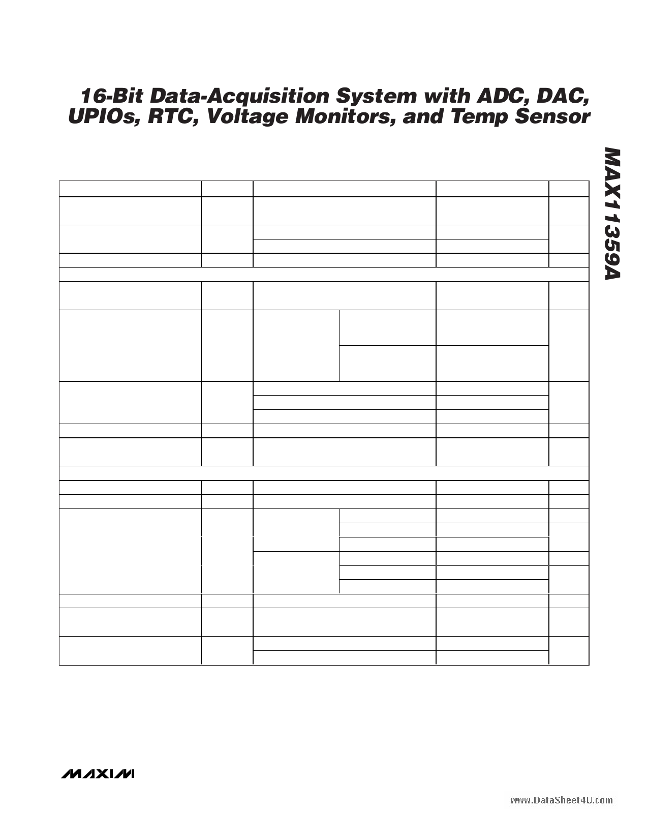
ELECTRICAL CHARACTERISTICS (continued)
(AVDD = DVDD = +1.8V to +3.6V, VREF = +1.25V, external reference, CLK32K = 32.768kHz (external clock), CREG = 10µF, CCPOUT =
10µF, 10µF between CF+ and CF-, TA = TMIN to TMAX, unless otherwise noted. Typical values are at TA = +25°C.) (Note 1)
PARAMETER
SYMBOL
CONDITIONS
Long-Term Stability
(Note 9)
Output Noise Voltage
Turn-On Settling Time
TEMPERATURE SENSOR
Temperature Measurement
Resolution
Internal Temperature-Sensor
Measurement Error
External Temperature-Sensor
Measurement Error (Note 10)
Temperature Measurement Noise
Temperature Measurement
Power-Supply Rejection Ratio
OP AMP (RL = 10kΩ connected to AVDD/2)
Input Offset Voltage
VOS
Offset-Error Tempco
Input Bias Current (Note 7)
IBIAS
Input Offset Current
Input Common-Mode Voltage
Range
Common-Mode Rejection Ratio
IOS
CMVR
CMRR
f = 0.1Hz to 10Hz, AVDD = 3V
f = 10Hz to 10kHz, AVDD = 3V
Buffer only, settle to 0.1% of final value
ADC resolution is 16-bit, 10sps
Internal voltage
reference, four-
current calibration,
and stored
calibration
coefficients
TA = 0°C to +50°C
TA = -40oC to +85°C
TA = +25°C
TA = 0°C to +50°C
TA = -40°C to +85°C
VCM = 0.5V
TA = -40°C to +85°C
IN1+, IN2+, IN3+ TA = 0°C to +70°C
TA = 0°C to +50°C
TA = -40°C to +85°C
IN1-, IN2-, IN3-
TA = 0°C to +70°C
TA = 0°C to +50°C
VIN1_, VIN2_ = +0.3V to (AVDD - 0.3V) (Note 7)
0 ≤ VCM ≤ 75mV
75mV < VCM ≤ AVDD - 0.35V, TA = +25°C
MIN
0
60
TYP
35
50
400
100
MAX
UNITS
ppm/
1000hrs
µVP-P
µs
0.11
±0.5
±1
±0.50
±0.5
±1.0
0.18
0.2
°C/LSB
°C
°C
°CRMS
°C/V
3
0.006
4
2
0.025
20
60
75
±15
±1
±300
±200
±1
±600
±400
±1
AVDD -
0.35
mV
µV/oC
nA
pA
nA
pA
nA
V
dB
_______________________________________________________________________________________ 5
5 Page 
www.DataSheet4U.com
16-Bit Data-Acquisition System with ADC, DAC,
UPIOs, RTC, Voltage Monitors, and Temp Sensor
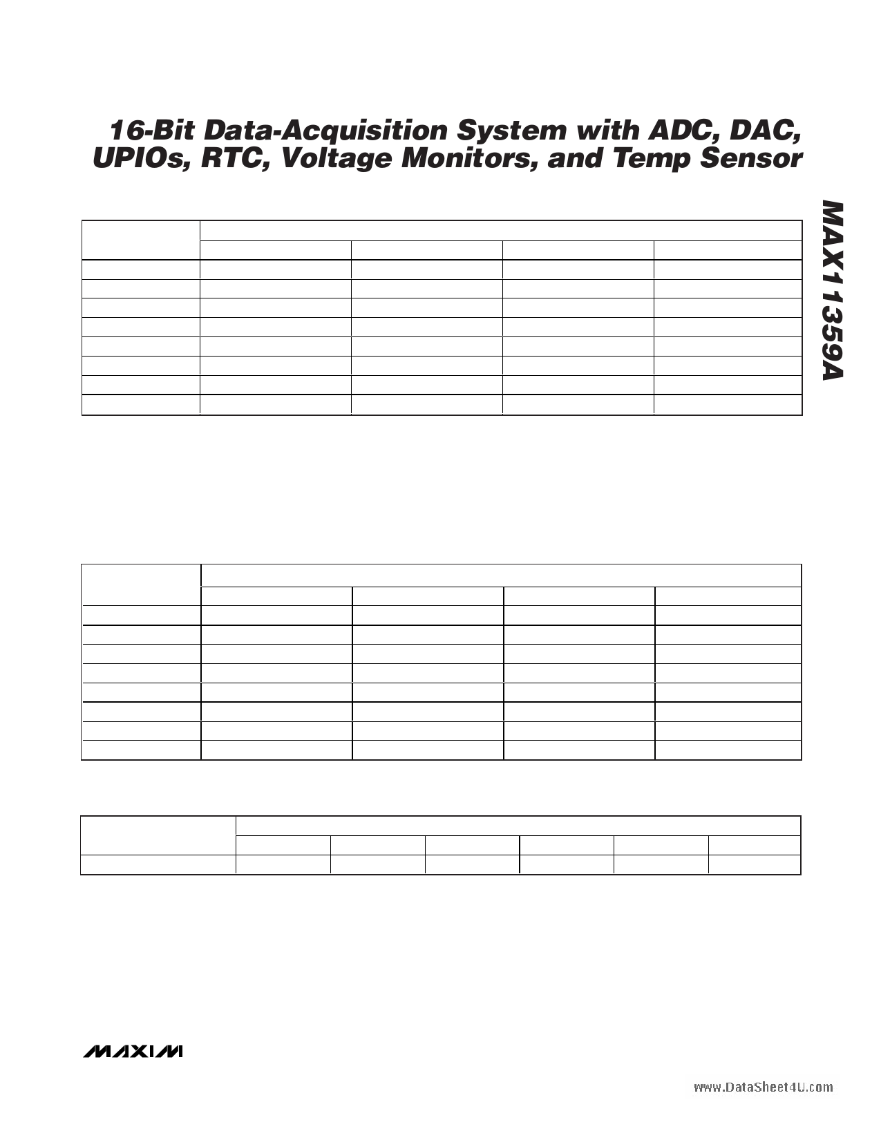
Table 1. Output Noise (Notes 12, 13, and 14)
RATE (sps)
10
40
50
60
200
240
400
512
GAIN = 1
1.684
3.178
3.234
3.307
55.336
104.596
587.138
983.979
OUTPUT NOISE (µVRMS)
GAIN = 2
GAIN = 4
1.684
1.684
3.178
3.178
3.234
3.234
3.307
3.307
55.336
55.336
104.596
104.596
587.138
587.138
983.979
983.979
GAIN = 8
1.684
3.178
3.234
3.307
55.336
104.596
587.138
983.979
Note 12: VREF = ±1.25V, bipolar mode, VIN = 1.24912V, PGA gain = 1, TA = +85°C.
Note 13: CIN = 5pF, op-amp noise is considered to be the same as the switching noise. The increase of the op amp’s noise contri-
bution is due to a large input swing (0 to 3.6V).
Note 14: Assume ±3 sigma peak-to-peak variation; noise-free resolution means no code flicker at given bits’ LSB.
Table 2. Peak-to-Peak Resolution
RATE (sps)
10
40
50
60
200
240
400
512
GAIN = 1
17.49
16.57
16.55
16.51
12.45
11.53
9.04
8.30
PEAK-TO-PEAK RESOLUTION (BITS)
GAIN = 2
GAIN = 4
17.49
17.49
16.57
16.57
16.55
16.55
16.51
16.51
12.45
12.45
11.53
11.53
9.04 9.04
8.30 8.30
GAIN = 8
17.49
16.57
16.55
16.51
12.45
11.53
9.04
8.30
Table 3. Maximum External Source Impedance Without 16-Bit Gain Error
PARAMETER
0 (Note 15)
EXTERNAL CAPACITANCE (pF)
50 100 500 1000
Resistance (kΩ)
350 60 30 10
4
Note 15: 2pF parasitic capacitance is assumed, which represents pad and any other parasitic capacitance.
5000
1
______________________________________________________________________________________ 11
11 Page | ||
| Páginas | Total 30 Páginas | |
| PDF Descargar | [ Datasheet MAX11359A.PDF ] | |
Hoja de datos destacado
| Número de pieza | Descripción | Fabricantes |
| MAX11359A | Data-Acquisition System | Maxim Integrated Products |
| Número de pieza | Descripción | Fabricantes |
| SLA6805M | High Voltage 3 phase Motor Driver IC. |
Sanken |
| SDC1742 | 12- and 14-Bit Hybrid Synchro / Resolver-to-Digital Converters. |
Analog Devices |
|
DataSheet.es es una pagina web que funciona como un repositorio de manuales o hoja de datos de muchos de los productos más populares, |
| DataSheet.es | 2020 | Privacy Policy | Contacto | Buscar |
