|
|
|
PDF 8951 Data sheet ( Hoja de datos )
| Número de pieza | 8951 | |
| Descripción | 8-Bit Microcontroller | |
| Fabricantes | ATMEL Corporation | |
| Logotipo | ||
Hay una vista previa y un enlace de descarga de 8951 (archivo pdf) en la parte inferior de esta página. Total 15 Páginas | ||
|
No Preview Available !
www.DataSheet4U.com
Features
• Compatible with MCS-51™ Products
• 4 Kbytes of In-System Reprogrammable Flash Memory
Endurance: 1,000 Write/Erase Cycles
Fully Static Operation: 0 Hz to 24 MHz
• Three-Level Program Memory Lock
• 128 x 8-Bit Internal RAM
• 32 Programmable I/O Lines
• Two 16-Bit Timer/Counters
• Six Interrupt Sources
• Programmable Serial Channel
•• Low Power Idle and Power Down Modes
Description
The AT89C51 is a low-power, high-performance CMOS 8-bit microcomputer with 4
Kbytes of Flash Programmable and Erasable Read Only Memory (PEROM). The
device is manufactured using Atmel’s high density nonvolatile memory technology
and is compatible with the industry standard MCS-51™ instruction set and pinout.
The on-chip Flash allows the program memory to be reprogrammed in-system or by
a conventional nonvolatile memory programmer. By combining a versatile 8-bit CPU
with Flash on a monolithic chip, the Atmel AT89C51 is a powerful microcomputer
which provides a highly flexible and cost effective solution to many embedded control
applications.
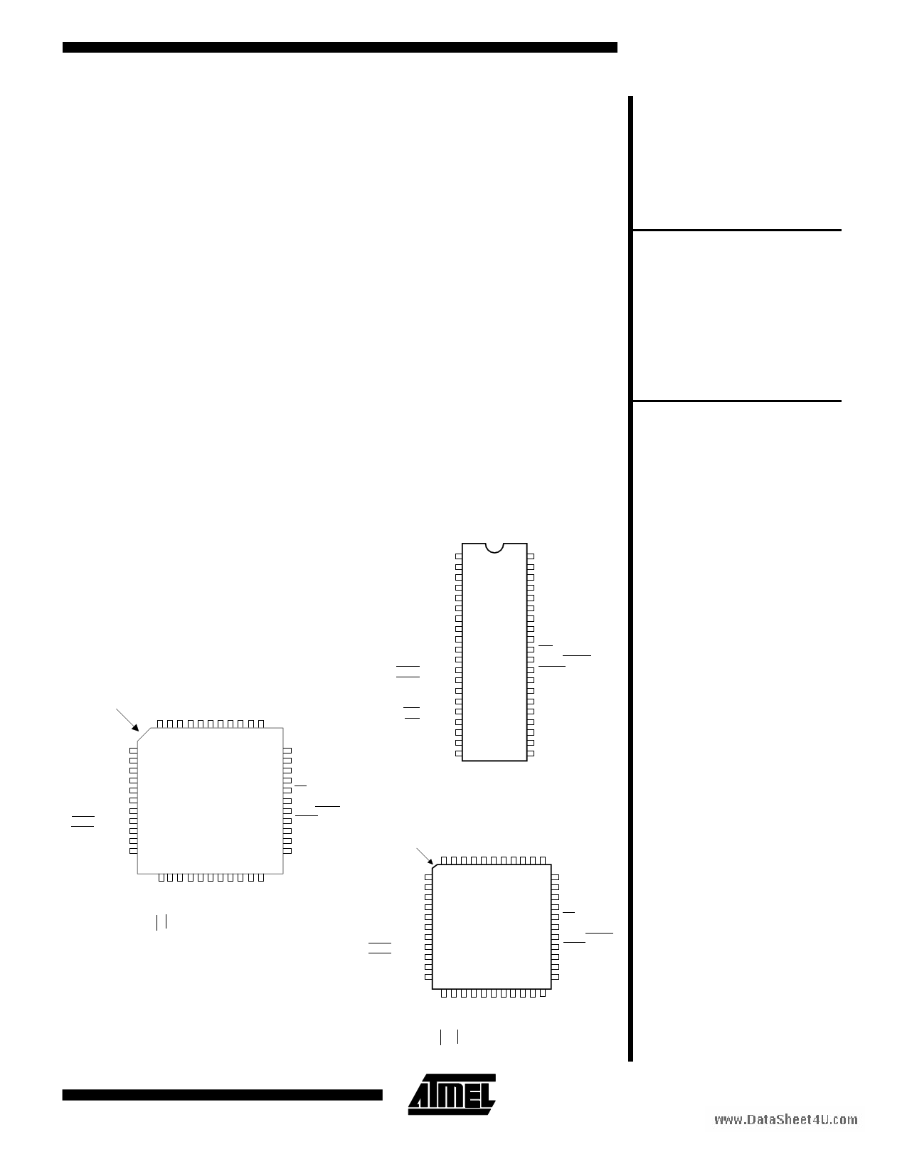
Pin Configurations
(continued)
PDIP/Cerdip
INDEX
CORNER
P1.5
P1.6
P1.7
RST
(RXD) P3.0
NC
(TXD) P3.1
(INT0) P3.2
(INT1) P3.3
(T0) P3.4
(T1) P3.5
PQFP/TQFP
4 44 34 24 14 03 93 83 73 63 53 4
1 33
2 32
3 31
4 30
5 29
6 28
7 27
8 26
9 25
10 24
11 23
1
21
31
41
51
61
71
1
8
9
2
0
2
12
2
P0.4 (AD4)
P0.5 (AD5)
P0.6 (AD6)
P0.7 (AD7)
EA/VPP
NC
ALE/PROG
PSEN
P2.7 (A15)
P2.6 (A14)
P2.5 (A13)
P1.0
P1.1
P1.2
P1.3
P1.4
P1.5
P1.6
P1.7
RST
(RXD) P3.0
(TXD) P3.1
(INT0) P3.2
(INT1) P3.3
(T0) P3.4
(T1) P3.5
(WR) P3.6
(RD) P3.7
X TA L 2
X TA L 1
GND
1
2
3
4
5
6
7
8
9
10
11
12
13
14
15
16
17
18
19
20
40 VCC
39 P0.0 (AD0)
38 P0.1 (AD1)
37 P0.2 (AD2)
36 P0.3 (AD3)
35 P0.4 (AD4)
34 P0.5 (AD5)
33 P0.6 (AD6)
32 P0.7 (AD7)
31 EA/VPP
30 ALE/PROG
29 PSEN
28 P2.7 (A15)
27 P2.6 (A14)
26 P2.5 (A13)
25 P2.4 (A12)
24 P2.3 (A11)
23 P2.2 (A10)
22 P2.1 (A9)
21 P2.0 (A8)
PLCC/LCC
INDEX
CORNER
P1.5
P1.6
P1.7
RST
(RXD) P3.0
NC
(TXD) P3.1
(INT0) P3.2
(INT1) P3.3
(T0) P3.4
(T1) P3.5
6 4 2 44 42 40
7 5 3 1 43 4139
8 38
9 37
10 36
11 35
12 34
13 33
14 32
15 31
16 30
11781 92 02 12 22 32 42 52 62 72289
P0.4 (AD4)
P0.5 (AD5)
P0.6 (AD6)
P0.7 (AD7)
EA/VPP
NC
ALE/PROG
PSEN
P2.7 (A15)
P2.6 (A14)
P2.5 (A13)
8-Bit
Microcontroller
with 4 Kbytes
Flash
AT89C51
0265E
1 page 
AT89C51
www.DataSheet4U.com
ware inhibits access to internal RAM in this event, but ac-
cess to the port pins is not inhibited. To eliminate the pos-
sibility of an unexpected write to a port pin when Idle is
terminated by reset, the instruction following the one that
invokes Idle should not be one that writes to a port pin or
to external memory.
Power Down Mode
In the power down mode the oscillator is stopped, and the
instruction that invokes power down is the last instruction
executed. The on-chip RAM and Special Function Regis-
ters retain their values until the power down mode is termi-
nated. The only exit from power down is a hardware reset.
Reset redefines the SFRs but does not change the on-
chip RAM. The reset should not be activated before VCC
is restored to its normal operating level and must be held
active long enough to allow the oscillator to restart and
stabilize.
Program Memory Lock Bits
On the chip are three lock bits which can be left unpro-
grammed (U) or can be programmed (P) to obtain the ad-
ditional features listed in the table below:
When lock bit 1 is programmed, the logic level at the EA
pin is sampled and latched during reset. If the device is
powered up without a reset, the latch initializes to a ran-
dom value, and holds that value until reset is activated. It
is necessary that the latched value of EA be in agreement
with the current logic level at that pin in order for the device
to function properly.
Lock Bit Protection Modes
Program Lock Bits
LB1 LB2 LB3
1 UUU
2 PUU
3 PPU
4PPP
Protection Type
No program lock features.
MOVC instructions executed from external program memory are disabled from
fetching code bytes from internal memory, EA is sampled and latched on reset, and
further programming of the Flash is disabled.
Same as mode 2, also verify is disabled.
Same as mode 3, also external execution is disabled.
Programming the Flash
The AT89C51 is normally shipped with the on-chip Flash
memory array in the erased state (that is, contents = FFH)
and ready to be programmed. The programming interface
accepts either a high-voltage (12-volt) or a low-voltage
(VCC) program enable signal. The low voltage program-
ming mode provides a convenient way to program the
AT89C51 inside the user’s system, while the high-voltage
programming mode is compatible with conventional third
party Flash or EPROM programmers.
The AT89C51 is shipped with either the high-voltage or
low-voltage programming mode enabled. The respective
top-side marking and device signature codes are listed in
the following table.
Top-Side Mark
Signature
VPP = 12 V
AT89C51
xxxx
yyww
(030H)=1EH
(031H)=51H
(032H)=FFH
VPP = 5 V
AT89C51
xxxx-5
yyww
(030H)=1EH
(031H)=51H
(032H)=05H
The AT89C51 code memory array is programmed byte-
by-byte in either programming mode. To program any
non-blank byte in the on-chip Flash Memory, the entire
memory must be erased using the Chip Erase Mode.
Programming Algorithm: Before programming the
AT89C51, the address, data and control signals should be
set up according to the Flash programming mode table
and Figures 3 and 4. To program the AT89C51, take the
following steps.
1. Input the desired memory location on the address
lines.
2. Input the appropriate data byte on the data lines.
3. Activate the correct combination of control signals.
4. Raise EA/VPP to 12 V for the high-voltage program-
ming mode.
5. Pulse ALE/PROG once to program a byte in the Flash
array or the lock bits. The byte-write cycle is self-timed and
typically takes no more than 1.5 ms. Repeat steps 1
through 5, changing the address and data for the entire
array or until the end of the object file is reached.
Data Polling: The AT89C51 features Data Polling to indi-
cate the end of a write cycle. During a write cycle, an at-
5
(continued)
5 Page 
www.DataSheet4U.com
External Program Memory Read Cycle
AT89C51
ALE
PSEN
PORT 0
PORT 2
tLHLL
tAVLL
tLLPL
tLLAX
A0 - A7
tPLAZ
tLLIV
tPLIV
tPXIZ
tPXIX
INSTR IN
tPLPH
tPXAV
tAVIV
A8 - A15
A0 - A7
A8 - A15
External Data Memory Read Cycle
ALE
PSEN
RD
PORT 0
PORT 2
tLHLL
tAVLL
tLLDV
tLLWL
tLLAX
tRLAZ
tRLRH
tRLDV
A0 - A7 FROM RI OR DPL
DATA IN
tAVWL
tAVDV
P2.0 - P2.7 OR A8 - A15 FROM DPH
tWHLH
tRHDZ
tRHDX
A0 - A7 FROM PCL
INSTR IN
A8 - A15 FROM PCH
11
11 Page | ||
| Páginas | Total 15 Páginas | |
| PDF Descargar | [ Datasheet 8951.PDF ] | |
Hoja de datos destacado
| Número de pieza | Descripción | Fabricantes |
| 8951 | 8-Bit Microcontroller | ATMEL Corporation |
| 8958 | VOICE COIL MOTOR DRIVER | Allegro MicroSystems |
| Número de pieza | Descripción | Fabricantes |
| SLA6805M | High Voltage 3 phase Motor Driver IC. |
Sanken |
| SDC1742 | 12- and 14-Bit Hybrid Synchro / Resolver-to-Digital Converters. |
Analog Devices |
|
DataSheet.es es una pagina web que funciona como un repositorio de manuales o hoja de datos de muchos de los productos más populares, |
| DataSheet.es | 2020 | Privacy Policy | Contacto | Buscar |