|
|
|
PDF MAX13330 Data sheet ( Hoja de datos )
| Número de pieza | MAX13330 | |
| Descripción | (MAX13330 / MAX13331) Automotive DirectDrive Headphone Amplifiers | |
| Fabricantes | Maxim Integrated Products | |
| Logotipo | ||
Hay una vista previa y un enlace de descarga de MAX13330 (archivo pdf) en la parte inferior de esta página. Total 15 Páginas | ||
|
No Preview Available !
19-4341; Rev 0; 10/08
www.DataSheet4U.com
Automotive DirectDrive Headphone Amplifiers
with Output Protection and Diagnostics
General Description
The MAX13330/MAX13331 stereo headphone amplifiers
are designed for automotive applications requiring out-
put short-circuit and ESD protection to battery/ground
with diagnostics. These devices use Maxim’s unique,
patented† DirectDrive® architecture to produce a
ground-referenced output from a single supply, elimi-
nating the need for large DC-blocking capacitors, sav-
ing board space and component height. The gain of the
amplifier is set internally (-1.5V/V) on the MAX13330 or
adjusted externally with resistors on the MAX13331.
The MAX13330/MAX13331 deliver 120mW per channel
into a 16Ω load or 135mW into a 32Ω load and have a
low 0.01% THD+N. Low output impedance and the effi-
cient integrated charge pump allows the device to drive
loads as low as 8Ω, enabling the use of small loud-
speakers. An 80dB at 217Hz PSRR allows these
devices to operate from noisy digital supplies without
an additional linear regulator. These devices include
±15kV Human Body Model ESD protection and short-
circuit protection up to +45V at the headphone outputs.
Comprehensive click-and-pop circuitry suppresses
audible clicks and pops on startup and shutdown. A
low-power shutdown mode reduces the supply current
to 3µA (typ).
The MAX13330/MAX13331 are specified from -40°C to
+105°C AEC-Q100 Level 2 automotive temperature
range and are available in a 16-pin QSOP package.
Applications
Automotive Entertainment Systems
Automotive Rear Seat Entertainment Systems
DirectDrive is a registered trademark of Maxim Integrated
Products, Inc.
†U.S. Patent #7,061,327
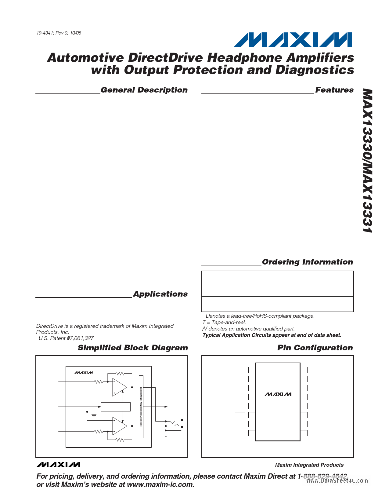
Simplified Block Diagram
Features
♦ 4V to 5.5V Single-Supply Operation
♦ 2MHz Charge Pump Prevents AM Radio
Interference
♦ Ground-Referenced Outputs Eliminate Bulky DC-
Blocking Capacitors
♦ Short-to-Ground and Battery (VBAT up to +45V)
Output Protection, Load Dump Protection
♦ Short-Circuit Diagnostic Output
♦ Adjustable Gain (MAX13331) or Fixed -1.5V/V Gain
(MAX13330)
♦ 135mW per Channel into 32Ω at 1% THD+N
♦ Low 0.01% THD+N
♦ Integrated Click-and-Pop Suppression
♦ High PSRR Eliminates LDO
♦ No Degradation of Low-Frequency Response Due
to Output Capacitors
♦ ±15kV Human Body Model ESD Protection for
Output Pins
Ordering Information
PART
GAIN
TEMP
RANGE
PIN-
PACKAGE
MAX13330GEE/V+T -1.5V/V -40°C to +105°C 16 QSOP
MAX13331GEE/V+T
Externally
Set
-40°C to +105°C
16 QSOP
+Denotes a lead-free/RoHS-compliant package.
T = Tape-and-reel.
/V denotes an automotive qualified part.
Typical Application Circuits appear at end of data sheet.
Pin Configuration
LEFT-CHANNEL
AUDIO IN
MAX13330
SHDN
RIGHT-CHANNEL
AUDIO IN
CLICK-AND-POP
SUPPRESSION
DIAGNOSTICS
OUTPUT
INL 1 +
SGND 2
INR 3
SGND 4
VDD 5
SHDN 6
CPVDD 7
C1P 8
MAX13330
MAX13331
16 OUTL
15 PGND
14 VSS
13 OUTR
12 DIAG
11 CPVSS
10 C1N
9 PGND
QSOP
________________________________________________________________ Maxim Integrated Products 1
For pricing, delivery, and ordering information, please contact Maxim Direct at 1-888-629-4642,
or visit Maxim’s website at www.maxim-ic.com.
1 page 
www.DataSheet4U.com
Automotive DirectDrive Headphone Amplifiers
with Output Protection and Diagnostics
Typical Operating Characteristics (continued)
(VDD = VCPVDD = 5V, VSGND = VPGND = 0, C1 = C2 = 1µF, RL = ∞, gain = -1.5V/V, THD+N measurement bandwidth = 22Hz to 22kHz,
TA = +25°C, unless otherwise noted.)
TOTAL HARMONIC DISTORTION
PLUS NOISE vs. OUTPUT POWER
10
VDD = 5V
RL = 16Ω
1
fIN = 10kHz
fIN = 1kHz
0.1
TOTAL HARMONIC DISTORTION
PLUS NOISE vs. OUTPUT POWER
10
VDD = 4V
RL = 32Ω
1
fIN = 10kHz
0.1 fIN = 1kHz
TOTAL HARMONIC DISTORTION
PLUS NOISE vs. OUTPUT POWER
10
VDD = 5V
RL = 32Ω
1
fIN = 10kHz
0.1 fIN = 1kHz
0.01 0.01 0.01
0.001
0
fIN = 100Hz
25 50 75 100 125 150 175
OUTPUT POWER (mW)
0.001
0
fIN = 100Hz
25 50 75 100
OUTPUT POWER (mW)
125
0.001
0
fIN = 100Hz
25 50 75 100 125 150 175
OUTPUT POWER (mW)
TOTAL HARMONIC DISTORTION
PLUS NOISE vs. FREQUENCY
1
VDD = 5V
RL = 1kΩ
0.1 VOUT_ = 2VRMS
0.01 VOUT_ = 1VRMS
0.001
0.0001
0.01
0.1 1 10
FREQUENCY (kHz)
100
OUTPUT POWER vs. SUPPLY VOLTAGE
180
160
fIN = 1kHz
1% THD+N
140
120 RL = 32Ω
100
80 RL = 16Ω
60
RL = 8Ω
40
20
0
4.00
4.25 4.50 4.75 5.00 5.25
SUPPLY VOLTAGE (V)
5.50
OUTPUT POWER vs. LOAD RESISTANCE
200
180 fIN = 1kHz
160
10% THD+N
VDD = 5V
140 1% THD+N
120 VDD = 5V
100
10% THD+N
VDD = 4V
80
60
40 1% THD+N
20 VDD = 4V
0
0 10 100 1000
LOAD RESISTANCE (Ω)
POWER DISSIPATION vs.
OUTPUT POWER PER CHANNEL
800
VDD = 4V
700 fIN = 1kHz
600 RL = 8Ω
500
RL = 16Ω
400
300
200
RL = 32Ω
100
0
0 20 40 60 80 100 120
OUTPUT POWER PER CHANNEL (mW)
POWER DISSIPATION vs.
OUTPUT POWER PER CHANNEL
1200
VDD = 5V
1000 fIN = 1kHz
RL = 8Ω
800
RL = 16Ω
600
400
200 RL = 32Ω
0
0 20 40 60 80 100 120 140 160 180
OUTPUT POWER PER CHANNEL (mW)
_______________________________________________________________________________________ 5
5 Page 
www.DataSheet4U.com
Automotive DirectDrive Headphone Amplifiers
with Output Protection and Diagnostics
Thermal-overload protection limits total power dissipa-
tion in the MAX13330/MAX13331. When the junction
temperature exceeds +145°C (typ), the thermal-protec-
tion circuitry disables the amplifier output stage. The
amplifiers are enabled once the junction temperature
cools by 5°C. This results in a pulsing output under
continuous thermal-overload conditions.
Output Power
The device has been specified for the worst-case sce-
nario, when both inputs are in-phase. Under this condi-
tion, the amplifiers simultaneously draw current from the
charge pump, leading to a proportional reduction in
VSS headroom. In typical stereo audio applications, the
left and right signals have differences in both magni-
tude and phase, subsequently leading to an increase in
the maximum attainable output power. Figure 4 shows
the two extreme cases for in- and out-of-phase. In reali-
ty, the available power lies between these extremes.
OUTPUT POWER vs. SUPPLY VOLTAGE
250
200
fIN = 1kHz
RL = 32Ω
THD+N = 10%
INPUTS 180°
OUT OF PHASE
150
INPUTS
IN PHASE
100
50
0
4.00
4.25 4.50 4.75 5.00 5.25
SUPPLY VOLTAGE (V)
5.50
Figure 4. Output Power vs. Supply Voltage
UVLO
The MAX13330/MAX13331 feature a UVLO function that
prevents the device from operating if the supply voltage
is less than 3.6V (typ). This feature ensures proper
operation during brownout conditions and prevents
deep battery discharge. Once the supply voltage
reaches the UVLO threshold, the charge-pump is
turned on and the amplifiers are powered.
Component Selection
Gain-Setting Resistors (MAX13331 Only)
The gain of the MAX13330 is internally set at -1.5V/V.
All gain-setting resistors are integrated into the device,
reducing external component count. The internally set
gain, in combination with DirectDrive, results in a head-
phone amplifier that requires only five tiny 1µF capaci-
tors to complete the amplifier circuit: two for the
charge-pump, two for audio input coupling, and one for
power-supply bypassing (see the Typical Application
Circuits). The gain of the MAX13331 amplifier is set
externally as shown in the Typical Application Circuits,
the gain is:
AV
=
− RF
RIN
(V / V)
Choose feedback resistor values of 10kΩ. Values other
than 10kΩ increase output offset voltage due to the
input bias current, which in turn, increases the amount
of DC current flow to the load.
Input Filtering
The input capacitor (CIN), in conjunction with the input
resistor (RIN), forms a highpass filter that removes the
DC bias from an incoming signal (see the Typical
Application Circuits). The AC-coupling capacitor allows
the device to bias the signal to an optimum DC level.
Assuming zero source impedance, the -3dB point of
the highpass filter is given by:
f−3dB
=
2π
1
× RIN
×
CIN
(Hz)
Choose CIN so f-3dB is well below the lowest frequency
of interest. For the MAX13330, use the value of RIN as
given in the Electrical Characteristics table. Setting
f-3dB too high affects the device’s low-frequency
response. Use capacitors whose dielectrics have low-
voltage coefficients, such as tantalum or aluminum
electrolytic. Capacitors with high-voltage coefficients,
such as ceramics, can result in increased distortion at
low frequencies.
Charge-Pump Capacitor Selection
Use capacitors with an ESR less than 100mΩ for opti-
mum performance. Low-ESR ceramic capacitors mini-
mize the output resistance of the charge pump. For
best performance over the extended temperature
range, select capacitors with an X7R dielectric.
______________________________________________________________________________________ 11
11 Page | ||
| Páginas | Total 15 Páginas | |
| PDF Descargar | [ Datasheet MAX13330.PDF ] | |
Hoja de datos destacado
| Número de pieza | Descripción | Fabricantes |
| MAX1333 | (MAX1332 / MAX1333) True-Differential 12-Bit ADCs | Maxim Integrated Products |
| MAX13330 | (MAX13330 / MAX13331) Automotive DirectDrive Headphone Amplifiers | Maxim Integrated Products |
| MAX13330 | (MAX13330 / MAX13331) Automotive DirectDrive Headphone Amplifiers | Maxim Integrated Products |
| MAX13331 | (MAX13330 / MAX13331) Automotive DirectDrive Headphone Amplifiers | Maxim Integrated Products |
| Número de pieza | Descripción | Fabricantes |
| SLA6805M | High Voltage 3 phase Motor Driver IC. |
Sanken |
| SDC1742 | 12- and 14-Bit Hybrid Synchro / Resolver-to-Digital Converters. |
Analog Devices |
|
DataSheet.es es una pagina web que funciona como un repositorio de manuales o hoja de datos de muchos de los productos más populares, |
| DataSheet.es | 2020 | Privacy Policy | Contacto | Buscar |