|
|
|
PDF MAX11040 Data sheet ( Hoja de datos )
| Número de pieza | MAX11040 | |
| Descripción | Sigma-Delta ADC | |
| Fabricantes | Maxim Integrated Products | |
| Logotipo | ||
Hay una vista previa y un enlace de descarga de MAX11040 (archivo pdf) en la parte inferior de esta página. Total 30 Páginas | ||
|
No Preview Available !
19-4302; Rev 0; 5/09
www.DataSheEeVtA4ALUVUA.AcILoTAImOBNLEKIT
24-Bit, 4-Channel, Simultaneous-Sampling,
Cascadable, Sigma-Delta ADC
General Description
The MAX11040 is a 24-bit, 4-channel, simultaneous-
sampling, sigma-delta analog-to-digital converter
(ADC). The device allows simultaneous sampling of as
many as 32 channels using a built-in cascade feature
to synchronize as many as eight devices. The serial
interface of the MAX11040 allows reading data from all
the cascaded devices using a single command. Four
modulators simultaneously convert each fully differen-
tial analog input with a programmable data output rate
ranging from 0.25ksps to 64ksps. The device achieves
106dB SNR at 16ksps and 117dB SNR at 1ksps. The
MAX11040 operates from a single +3V supply. The dif-
ferential analog input range is ±2.2V when using the
internal reference, an external reference is optional.
Each input is overvoltage protected up to ±6V without
damage. The device uses an internal crystal oscillator
or an external source for clock.
The MAX11040 is compatible with SPI™, QSPI™,
MICROWIRE™, and DSP-compatible 4-wire serial inter-
faces. An on-board interface logic allows one serial inter-
face (with a single chip select) to control up to eight
cascaded devices or 32 simultaneous sampling analog
input channels.
The MAX11040 is ideally suited for power-management
systems. Each channel includes an adjustable sam-
pling phase enabling internal compensation for phase
shift due to external dividers, transformers, or filters at
the inputs. The output data rate is adjustable with a
0.065% resolution (at 16ksps or below) to track the
varying frequency of a periodic input. A SYNC input
allows periodic alignment of the conversion timing of
multiple devices with a remote timing source.
The MAX11040 is available in a 38-pin TSSOP package
specified over the -40°C to +105°C industrial tempera-
ture range.
Applications
Power Protection Relay Equipment
Multiphase Power Systems
Industrial Data-Acquisition Systems
Medical Instrumentation
Ordering Information
PART
TEMP RANGE
PIN-PACKAGE
MAX11040GUU+ -40°C to +105°C
38 TSSOP
+Denotes a lead(Pb)-free/RoHS-compliant package.
MICROWIRE is a trademark of National Semiconductor Corp.
SPI/QSPI are trademarks of Motorola Inc.
Features
♦ Four Fully Differential Simultaneously Sampled
Channels
♦ Cascadable for Up to 32 Channels of
Simultaneous Sampling
♦ 106dB SNR at 16ksps
♦ 117dB SNR at 1ksps
♦ 0.25% Error Over a 1000:1 Dynamic Range,
Processed Over 16.7ms
♦ ±2.2V Full-Scale Input Range
♦ ±6V Overvoltage Protected Inputs
♦ Internal Crystal Oscillator
♦ 2.5V, 50ppm/°C Internal Reference or External
Reference
♦ Programmable Output Data Rate
0.25ksps to 64ksps Range
0.065% Resolution
♦ Programmable Sampling Phase
0 to 333µs Delay in 1.33µs Steps
♦ SPI-/QSPI-/MICROWIRE-/DSP-Compatible 4-Wire
Serial Interface
♦ Cascadable Interface Allows Control of Up to
Eight Devices with a Single CS Signal
♦ 3.0V to 3.6V Analog Supply Voltage
♦ 2.7V to VAVDD Digital Supply Voltage
♦ 38-Pin TSSOP Package
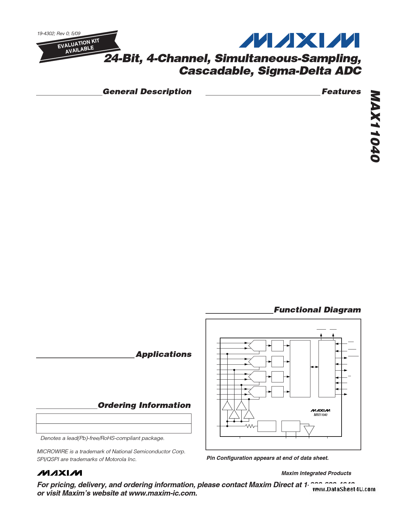
Functional Diagram
AIN0+
AIN0-
REF0
AIN1+
AIN1-
REF1
AIN2+
AIN2-
REF2
AIN3+
AIN3-
REF3
REFIO
24-BIT
ADC
24-BIT
ADC
24-BIT
ADC
24-BIT
ADC
OVRFLW FAULT
DIGITAL
FILTER
DIGITAL
FILTER
DIGITAL
FILTER
REGISTERS AND
DIGITAL
CONTROL
DIGITAL
FILTER
SERIAL
INTERFACE
SYNC
DRDYIN
DRDYOUT
CASCIN
CASCOUT
CS
SCLK
DIN
DOUT
AGND
2.5V
REFERENCE
CRYSTAL
OSCILLATOR
MAX11040
XIN XOUT CLKOUT
DGND
Pin Configuration appears at end of data sheet.
________________________________________________________________ Maxim Integrated Products 1
For pricing, delivery, and ordering information, please contact Maxim Direct at 1-888-629-4642,
or visit Maxim’s website at www.maxim-ic.com.
1 page 
www.DataSheet4U.com
24-Bit, 4-Channel, Simultaneous-Sampling,
Cascadable, Sigma-Delta ADC
ELECTRICAL CHARACTERISTICS (continued)
(VAVDD = +3.0V to +3.6V, VDVDD = +2.7V to VAVDD, fXIN CLOCK = 24.576MHz, fOUT = 16ksps, VREFIO = +2.5V (external), CREFIO =
CREF0 = CREF1 = CREF2 = CREF3 = 1µF to AGND, TA = TMIN to TMAX, unless otherwise noted. Typical values are at TA = +25°C.) (Note 1)
PARAMETER
SYMBOL
CONDITIONS
MIN TYP MAX UNITS
SYNC Pulse Width
tSYN
XIN
2 Clock
Cycles
XIN Clock Pulse Width
DRDYIN to DRDYOUT
XIN Clock to DRDYOUT Delay
XIN Clock Period
XIN Clock to SYNC Setup
SYNC to XIN Clock Hold
XIN to CLKOUT Delay
Power-On Reset Delay
tXPW
tDRDY
tXDRDY
tXP
tSS
tHS
tXCD
CLOAD = 30pF
DRDYIN = DGND
(Note 12)
(Note 12)
(Note 13)
16
20
40
40
16
5
40
<1
ns
ns
ns
ns
ns
ns
ns
ms
Note 1: Devices are production tested at +105°C. Specifications to -40°C are guaranteed by design.
Note 2: Tested at VAVDD = VDVDD = +3.0V.
Note 3: Integral nonlinearity is the deviation of the analog value at any code from its ideal value after the offset and gain errors are
removed.
Note 4: Offset nulled.
Note 5: Offset and gain drift defined as change in offset and gain error vs. full scale.
Note 6: Noise measured with AIN_+ = AIN_- = AGND.
Note 7: Relative accuracy is defined as the difference between the actual RMS amplitude and the ideal RMS amplitude of a 62.5Hz
sine wave, measured over one cycle at a 16ksps data rate, expressed as a fraction of the ideal RMS amplitude. The rela-
tive accuracy specification refers to the maximum error expected over 1 million measurements. Calculated from SNR. Not
production tested.
Note 8: Latency is a function of the sampling rate and XIN clock. See the Latency section in the Digital Filter section.
Note 9: Voltage levels below the positive fault threshold and above the negative fault threshold, relative to AGND on each individ-
ual AIN_+ and AIN_- input, do not trigger the analog input protection circuitry.
Note 10: Test performed using RXD MP35.
Note 11: All digital inputs at DGND or DVDD.
Note 12: SYNC is captured by the subsequent XIN clock if this specification is violated.
Note 13: Delay from DVDD exceeds 2.0V until digital interface is operational.
_______________________________________________________________________________________ 5
5 Page 
www.DataSheet4U.com
24-Bit, 4-Channel, Simultaneous-Sampling,
Cascadable, Sigma-Delta ADC
Digital Filter
The MAX11040 contains an on-chip digital lowpass fil-
ter that processes the data stream from each modulator
and generates the high-resolution output data. The low-
pass filter frequency response is determined by the
programmable output data rate. At the nominal 16ksps
output data rate, the -3dB bandwidth of the filter is
3.4kHz. The passband flatness is better than ±0.1dB
from 0 to 1.74kHz. The notches are located at 5.75kHz
and 7.195kHz. These frequencies scale linearly with the
output data rate. See Figure 2 and Table 1 for the fre-
quency response at different data rates.
1
0
-1
-2
-3
-4
-5
-6
0
0.4 0.8 0.12 0.16 0.20 0.24 0.28
fAIN/fSAMPLE
Figure 2. Digital Filter Response
Table 1. Bandwidth vs. Output Data Rate
OUTPUT DATA
RATE (ksps)
0.5
1
2
4
8
10
12
16
32
64
-3dB BANDWIDTH
(kHz)
0.11
0.21
0.42
0.85
1.69
2.11
2.54
3.38
6.78
13.5
-0.1dB BANDWIDTH
(kHz)
0.05
0.11
0.22
0.43
0.87
1.09
1.31
1.74
3.48
6.96
Since the transfer function of a digital filter is repeatable
and predictable, it is possible to correct for frequency-
dependent attenuation in downstream software. See
the Compensating for the Rolloff of the Digital Filter in a
Typical FFT Analysis section. The transfer function is
defined by the following equation:
( )Gain(fAIN
)
=
⎛
⎜
⎜
⎜
⎝⎜⎜
⎛
sin⎝⎜
π
×
fAIN
fSAMPLE
⎞
⎠⎟
⎛
sin⎝⎜
π
×
fAIN
fXINCLOCK
⎞
⎠⎟
⎞
⎟
⎟
⎟
⎠⎟⎟
3
FIR _ Gain(fAIN )
where:
Gain is the filter gain.
fAIN is the analog input frequency.
fSAMPLE is the programmed output data rate, nomi-
nally 16kHz.
fXINCLOCK is the clock frequency at XIN, nominally
24.576MHz.
FIR_Gain (fAIN) is the normalized gain of the FIR fil-
ter with the following filter coefficients, as a function
of the analog input frequency fAIN. These coeffi-
cients are applied at the output data rate:
+ 0.021484375
- 0.072265625
- 0.035156250
+ 0.304687500
+ 0.539062500
+ 0.304687500
- 0.035156250
- 0.072265625
+ 0.021484375
Latency
The digital filter determines the latency of the
MAX11040. Latency is defined as the time between the
effective point in time that a sample is taken and when
the resulting digital data is available for reading.
The latency of the converter is specified by the follow-
ing equation:
Latency = (6 x tDOUT) + (PHI x 1.3µs) + 30µs
where tDOUT is the data output period (inverse of the
programmed sample rate), determined by fXINCLOCK
and the selected output data rate, and PHI is the pro-
grammed sampling instant delay for the channel in
question (0 ≤ PHI ≤ 255). The latency is approximately
405µs at 16ksps.
______________________________________________________________________________________ 11
11 Page | ||
| Páginas | Total 30 Páginas | |
| PDF Descargar | [ Datasheet MAX11040.PDF ] | |
Hoja de datos destacado
| Número de pieza | Descripción | Fabricantes |
| MAX1104 | 8-Bit CODECs | Maxim Integrated |
| MAX11040 | Sigma-Delta ADC | Maxim Integrated Products |
| MAX11040K | (MAX11040K / MAX11060) Sigma-Delta ADCs | Maxim Integrated Products |
| MAX11041 | (MAX11041 / MAX11042) Wired Remote Controllers | Maxim Integrated Products |
| Número de pieza | Descripción | Fabricantes |
| SLA6805M | High Voltage 3 phase Motor Driver IC. |
Sanken |
| SDC1742 | 12- and 14-Bit Hybrid Synchro / Resolver-to-Digital Converters. |
Analog Devices |
|
DataSheet.es es una pagina web que funciona como un repositorio de manuales o hoja de datos de muchos de los productos más populares, |
| DataSheet.es | 2020 | Privacy Policy | Contacto | Buscar |