|
|
|
PDF RMWB04001 Data sheet ( Hoja de datos )
| Número de pieza | RMWB04001 | |
| Descripción | 4 GHZ Buffer Amp | |
| Fabricantes | Fairchild Semiconductor | |
| Logotipo | ||
Hay una vista previa y un enlace de descarga de RMWB04001 (archivo pdf) en la parte inferior de esta página. Total 7 Páginas | ||
|
No Preview Available !
www.DataSheet4U.com
June 2004
RMWB04001
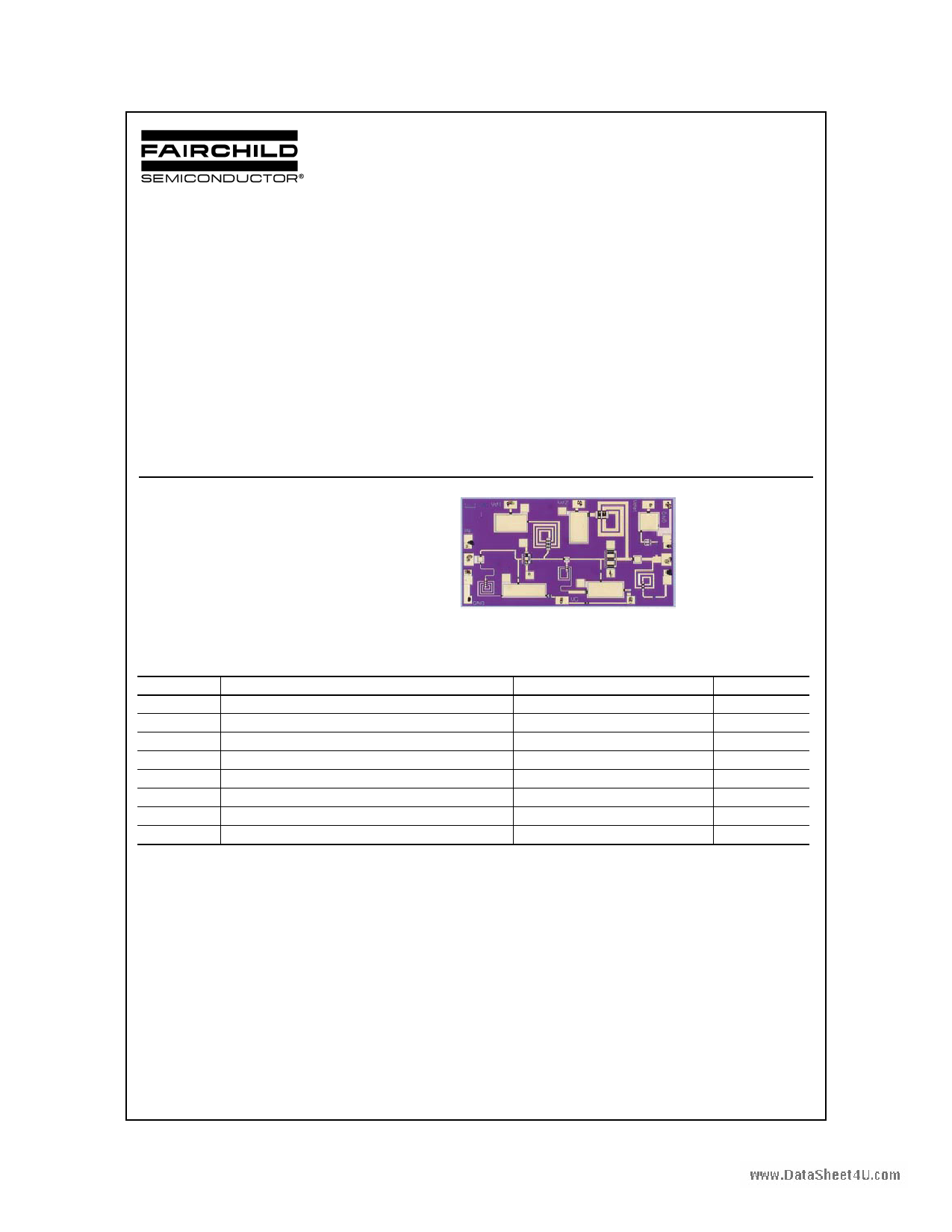
4 GHz Buffer Amplifier MMIC
General Description
The RMWB04001 is a 2-stage GaAs MMIC amplifier
designed as a 3.5 to 4 GHz Buffer Amplifier for use in point
to point and point to multi-point radios, and various
communications applications. In conjunction with other
amplifiers, multipliers and mixers it forms part of a complete
23 and 26 GHz transmit/receive chipset. The RMWB04001
utilizes our 0.25µm power PHEMT process and can be
used in a variety of applications requiring a high gain
medium power amplifier.
Features
• 4 mil substrate
• Small-signal gain 27dB (typ.)
• Saturated Power Out 20dBm (typ.)
• Voltage Detector Included to Monitor Pout
• Chip size 2.4mm x 1.3mm x 100µm
Device
Absolute Ratings
Symbol
Vd
Vg
Vdg
ID
PIN
TC
TSTG
RJC
Parameter
Positive DC Voltage (+4V Typical)
Negative DC Voltage
Simultaneous (Vd–Vg)
Positive DC Current
RF Input Power (from 50Ω source)
Operating Baseplate Temperature
Storage Temperature Range
Thermal Resistance (Channel to Backside)
Ratings
+6
-2
8
168
+7
-30 to +85
-55 to +125
140
Units
V
V
V
mA
dBm
°C
°C
°C/W
©2004 Fairchild Semiconductor Corporation
RMWB04001 Rev. C
1 page 
www.DataRSeheceot4Um.cmomended Procedure for Biasing and Operation
CAUTION: LOSS OF GATE VOLTAGE (Vg) WHILE
DRAIN VOLTAGE (Vd) IS PRESENT MAY DAMAGE THE
AMPLIFIER CHIP.
The following sequence of steps must be followed to
properly test the amplifier:
Step 1: Turn off RF input power.
Step 2: Connect the DC supply grounds to the ground of
the chip carrier. Slowly apply negative gate bias
supply voltage of -1.5V to Vg.
Step 3: Slowly apply positive drain bias supply voltage of
+4V to Vd.
Step 4: Adjust gate bias voltage to set the quiescent
current of Idq = 36mA.
Step 5: After the bias condition is established, the RF input
signal may now be applied at the appropriate
frequency band.
Step 6: Follow turn-off sequence of:
(i) Turn off RF input power,
(ii) Turn down and off drain voltage (Vd),
(iii) Turn down and off gate bias voltage (Vg).
©2004 Fairchild Semiconductor Corporation
RMWB04001 Rev. C
5 Page | ||
| Páginas | Total 7 Páginas | |
| PDF Descargar | [ Datasheet RMWB04001.PDF ] | |
Hoja de datos destacado
| Número de pieza | Descripción | Fabricantes |
| RMWB04001 | 4 GHZ Buffer Amp | Fairchild Semiconductor |
| Número de pieza | Descripción | Fabricantes |
| SLA6805M | High Voltage 3 phase Motor Driver IC. |
Sanken |
| SDC1742 | 12- and 14-Bit Hybrid Synchro / Resolver-to-Digital Converters. |
Analog Devices |
|
DataSheet.es es una pagina web que funciona como un repositorio de manuales o hoja de datos de muchos de los productos más populares, |
| DataSheet.es | 2020 | Privacy Policy | Contacto | Buscar |