|
|
|
PDF AAT2120 Data sheet ( Hoja de datos )
| Número de pieza | AAT2120 | |
| Descripción | 500mA Low Noise Step-Down Converter | |
| Fabricantes | Advanced Analogic Technologies | |
| Logotipo | ||
Hay una vista previa y un enlace de descarga de AAT2120 (archivo pdf) en la parte inferior de esta página. Total 19 Páginas | ||
|
No Preview Available !
SwitchRegTM
www.DataSheet4U.com
General Description
The AAT2120 SwitchReg is a 1.8MHz step-down con-
verter with an input voltage range of 2.7V to 5.5V and
output as low as 0.6V. Its low supply current, small size,
and high switching frequency make the AAT2120 the
ideal choice for portable applications.
The AAT2120 delivers up to 500mA of load current, while
maintaining a low 45μA no load quiescent current. The
1.8MHz switching frequency minimizes the size of exter-
nal components, while keeping switching losses low. The
AAT2120 feedback and control delivers excellent load
regulation and transient response with a small output
inductor and capacitor.
The AAT2120 maintains high efficiency throughout the
load range. The AAT2120’s unique architecture produces
reduced ripple and spectral noise. Over-temperature and
short-circuit protection safeguard the AAT2120 and sys-
tem components from damage.
The AAT2120 is available in a Pb-free, 8-pin, 2x2mm
STDFN package and is rated over the -40°C to +85°C
temperature range.
PRODUCT DATASHEET
AAT2120
500mA Low Noise Step-Down Converter
Features
• VIN Range: 2.7V to 5.5V
• VOUT Range: 0.6V to VIN
• Up to 500mA Output Current
• Up to 96% Efficiency
• Low Noise Light Load Mode
• 45μA Typical Quiescent Current
• 1.8MHz Switching Frequency
• Soft-Start Control
• Over-Temperature and Current Limit Protection
• 100% Duty Cycle Low-Dropout Operation
• <1μA Shutdown Current
• Small External Components
• Ultra-Small STDFN22-8 Package
• Temperature Range: -40°C to +85°C
Applications
• Bluetooth® Headsets
• Cellular Phones
• Digital Cameras
• Handheld Instruments
• Micro Hard Disk Drive
• Portable Music Players
• USB Devices
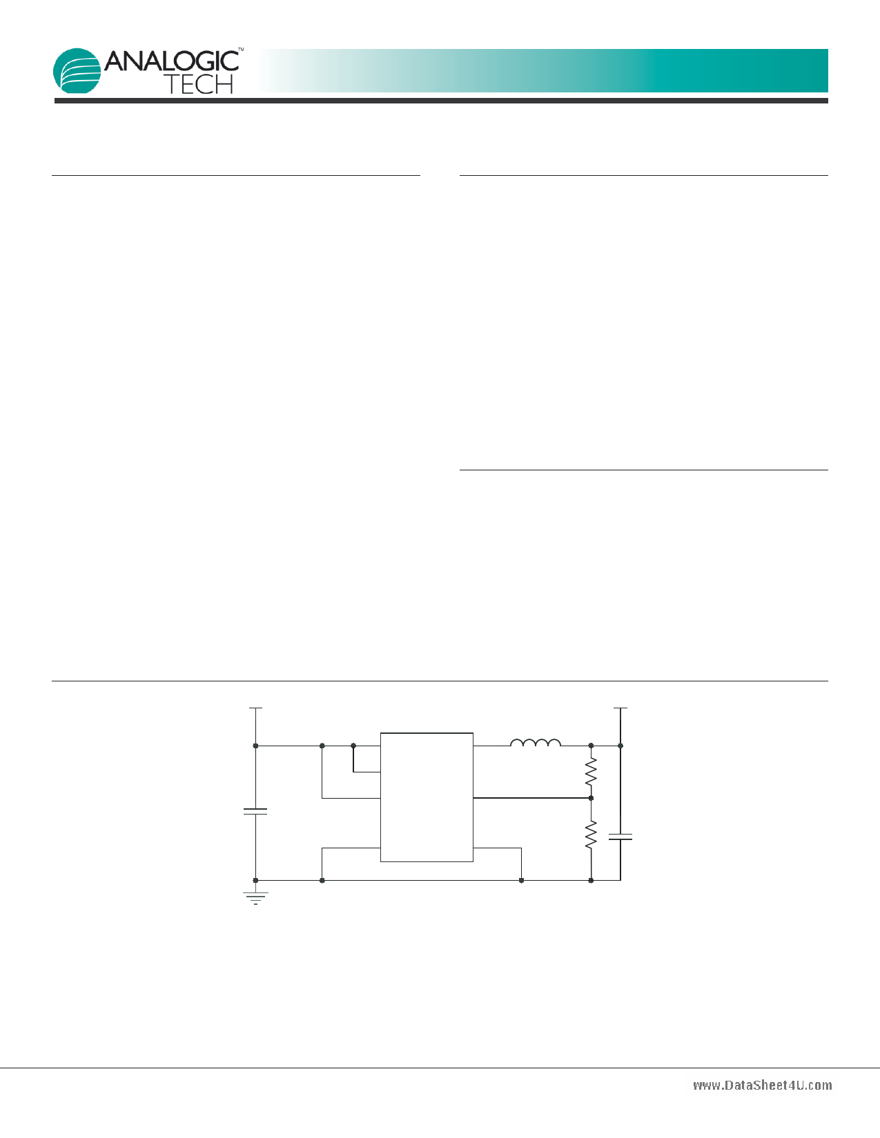
Typical Application
VIN
C1
4.7µF
AAT2120
VP LX
VIN
EN FB
GND PGND
VO = 1.8V
L1
3.0µH
R1
118kΩ
500mA
R2
59kΩ
C2
4.7µF
2120.2008.02.1.2
www.analogictech.com
1
1 page 
SwitchRegTM
www.DataSheet4U.com
Typical Characteristics
Efficiency vs. Load
(VOUT = 3.0V; L = 4.7µH)
100
90 VIN = 3.6V
80
VIN = 4.2V
70
60 VIN = 5.0V
50
40
0.1
1
10 100
Output Current (mA)
1000
Efficiency vs. Load
(VOUT = 1.8V; L = 3.3µH)
100
VIN = 2.7V
90
VIN = 3.6V
80
70 VIN = 4.2V
60
50
40
0.1
1 10 100
Output Current (mA)
1000
Efficiency vs. Load
(VOUT = 1.2V; L = 1.5µH)
100
90 VIN = 2.7V
80 VIN = 3.6V
70
60
50
VIN = 4.2V
VIN = 5.0V
40
0.1
1
10 100
Output Current (mA)
1000
PRODUCT DATASHEET
AAT2120
500mA Low Noise Step-Down Converter
1.0
0.8
0.6
0.4
0.2
0.0
-0.2
-0.4
-0.6
-0.8
-1.0
0.1
Load Regulation
(VOUT = 3.0V; L = 4.7µH)
VIN = 3.6V
VIN = 5.0V
VIN = 4.2V
1 10 100
Output Current (mA)
1000
1.0
0.8
0.6
0.4
0.2
0.0
-0.2
-0.4
-0.6
-0.8
-1.0
0.1
Load Regulation
(VOUT = 1.8V; L = 3.3µH)
VIN = 4.2V
VIN = 3.6V
VIN = 2.7V
1 10 100
Output Current (mA)
1000
Load Regulation
(VOUT = 1.2V; L = 1.5µH)
1.0
0.8 VIN = 2.7V
0.6
0.4 VIN = 3.6V
0.2
0.0
-0.2
-0.4
-0.6 VIN = 4.2V
-0.8
-1.0
0.1
1
10
VIN = 5.0V
100
Output Current (mA)
2120.2008.02.1.2
www.analogictech.com
5
5 Page 
SwitchRegTM
www.DataSheet4U.com
Output Voltage (V)
1.0
1.2
1.5
1.8
2.5
3.0
3.3
L1 (μH)
1.5
2.2
2.7
3.0
3.9
4.7
5.6
Table 1: Inductor Values.
The 3.0μH CDRH2D09 series inductor selected from
Sumida has a 150mΩ DCR and a 470mA DC current
rating. At full load, the inductor DC loss is 9.375mW
which gives a 2.08% loss in efficiency for a 250mA,
1.8V output.
Input Capacitor
Select a 4.7μF to 10μF X7R or X5R ceramic capacitor for
the input. To estimate the required input capacitor size,
determine the acceptable input ripple level (VPP) and solve
for CIN. The calculated value varies with input voltage and
is a maximum when VIN is double the output voltage.
VO · ⎛1 - VO ⎞
CIN =
VIN
⎛ VPP
⎝ IO
⎝ VIN ⎠
- ESR⎞⎠ · FS
VO
VIN
·
⎛⎝1 -
VO ⎞
VIN ⎠
=
1
4
for
VIN
=
2
·
VO
1
CIN(MIN) = ⎛ VPP
⎝ IO
- ESR⎞⎠ · 4 · FS
Always examine the ceramic capacitor DC voltage coeffi-
cient characteristics when selecting the proper value. For
example, the capacitance of a 10μF, 6.3V, X5R ceramic
capacitor with 5.0V DC applied is actually about 6μF.
The maximum input capacitor RMS current is:
IRMS = IO ·
VO · ⎛1 - VO ⎞
VIN ⎝ VIN ⎠
The input capacitor RMS ripple current varies with the
input and output voltage and will always be less than or
equal to half of the total DC load current.
PRODUCT DATASHEET
AAT2120
500mA Low Noise Step-Down Converter
VO · ⎛1 - VO ⎞ = D · (1 - D) = 0.52 = 1
VIN ⎝ VIN ⎠
2
for VIN = 2 · VO
I =RMS(MAX)
IO
2
VO · ⎛1 - VO ⎞
The term VIN ⎝ VIN ⎠ appears in both the input voltage
ripple and input capacitor RMS current equations and is
a maximum when VO is twice VIN. This is why the input
voltage ripple and the input capacitor RMS current ripple
are a maximum at 50% duty cycle.
The input capacitor provides a low impedance loop for
the edges of pulsed current drawn by the AAT2120. Low
ESR/ESL X7R and X5R ceramic capacitors are ideal for
this function. To minimize stray inductance, the capaci-
tor should be placed as closely as possible to the IC. This
keeps the high frequency content of the input current
localized, minimizing EMI and input voltage ripple.
The proper placement of the input capacitor (C1) can be
seen in the evaluation board layout in Figure 2.
A laboratory test set-up typically consists of two long
wires running from the bench power supply to the eval-
uation board input voltage pins. The inductance of these
wires, along with the low-ESR ceramic input capacitor,
can create a high Q network that may affect converter
performance. This problem often becomes apparent in
the form of excessive ringing in the output voltage dur-
ing load transients. Errors in the loop phase and gain
measurements can also result.
Since the inductance of a short PCB trace feeding the
input voltage is significantly lower than the power leads
from the bench power supply, most applications do not
exhibit this problem.
In applications where the input power source lead induc-
tance cannot be reduced to a level that does not affect
the converter performance, a high ESR tantalum or alu-
minum electrolytic should be placed in parallel with the
low ESR, ESL bypass ceramic. This dampens the high Q
network and stabilizes the system.
Output Capacitor
The output capacitor limits the output ripple and pro-
vides holdup during large load transitions. A 4.7μF to
10μF X5R or X7R ceramic capacitor typically provides
sufficient bulk capacitance to stabilize the output during
large load transitions and has the ESR and ESL charac-
teristics necessary for low output ripple. For enhanced
2120.2008.02.1.2
www.analogictech.com
11
11 Page | ||
| Páginas | Total 19 Páginas | |
| PDF Descargar | [ Datasheet AAT2120.PDF ] | |
Hoja de datos destacado
| Número de pieza | Descripción | Fabricantes |
| AAT2120 | Step-Down Converter | Skyworks |
| AAT2120 | 500mA Low Noise Step-Down Converter | Advanced Analogic Technologies |
| Número de pieza | Descripción | Fabricantes |
| SLA6805M | High Voltage 3 phase Motor Driver IC. |
Sanken |
| SDC1742 | 12- and 14-Bit Hybrid Synchro / Resolver-to-Digital Converters. |
Analog Devices |
|
DataSheet.es es una pagina web que funciona como un repositorio de manuales o hoja de datos de muchos de los productos más populares, |
| DataSheet.es | 2020 | Privacy Policy | Contacto | Buscar |