|
|
|
PDF IDT82V3155 Data sheet ( Hoja de datos )
| Número de pieza | IDT82V3155 | |
| Descripción | ENHANCED T1/E1/OC3 WAN PLL | |
| Fabricantes | Integrated Device Technology | |
| Logotipo | ||
Hay una vista previa y un enlace de descarga de IDT82V3155 (archivo pdf) en la parte inferior de esta página. Total 30 Páginas | ||
|
No Preview Available !
www.DataSheet4U.com
ENHANCED T1/E1/OC3 WAN PLL
WITH DUAL REFERENCE INPUTS
IDT82V3155
FEATURES
• Supports AT&T TR62411 and Telcordia GR-1244-CORE Stratum
3, Stratum 4 Enhanced and Stratum 4 clock, OC-3 port and
155.52 Mbit/s application
• Supports ITU-T G.813 Option 1 clocks
• Supports ITU-T G.812 Type IV clocks
• Supports ETSI ETS 300 011, TBR 4, TBR 12 and TBR 13 timing
for E1 interface
• Selectable reference inputs: 8 kHz, 1.544 MHz, 2.048 MHz or
19.44 MHz
• Accepts two independent reference inputs which may have
same or different nominal frequencies applied to them
• Provides C1.5o, C3o, C2o, C4o, C6o, C8o, C16o, C19o, C32o and
C155 output clock signals
• Provides 7 types of 8 kHz framing pulses: F0o, F8o, F16o, F19o,
F32o, RSP and TSP
• Provides a C2/C1.5 output clock signal with the frequency
controlled by the selected reference input Fref0 or Fref1
• Holdover frequency accuracy of 0.025 ppm
• Phase slope of 5 ns per 125 µs
• Attenuates wander from 2.1 Hz
• Fast lock mode
• Provides Time Interval Error (TIE) correction
• MTIE of 600 ns
• JTAG boundary scan
• Holdover status indication
• Freerun status indication
• Normal status indication
• Lock status indication
• Input reference quality indication
• 3.3 V operation with 5 V tolerant I/O
• Package available: 56-pin SSOP (Green option available)
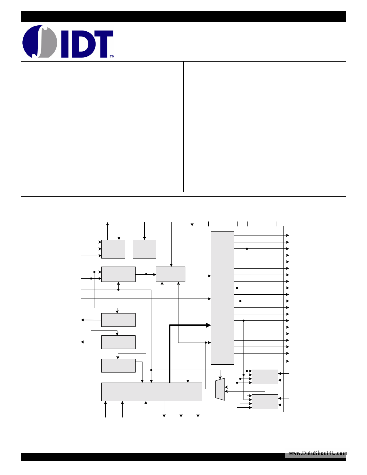
FUNCTIONAL BLOCK DIAGRAM
TDO TDI
OSCi
TCLR
RST
VDD VSS VDD VSS VDD VSS VDD VSS
TCK
TMS
TRST
Fref0
Fref1
IN_sel
FLOCK
MON_out0
MON_out1
JTAG
OSC
Reference Input
Switch
TIE Control
Block
Virtual
Reference
Reference Input
Monitor 0
Reference Input
Monitor 1
Invalid Input
Signal Detection
DPLL
Feedback Signal
State Control Circuit
Frequency
Select Circuit 0
Frequency
Select Circuit 1
C2/C1.5
C32o
C19o
C155POS
C155NEG
C16o
C8o
C4o
C2o
C3o
C1.5o
C6o
F0o
F8o
F16o
F19o
F32o
RSP
TSP
LOCK
F0_sel0
F0_sel1
F1_sel0
F1_sel1
TIE_en MODE_sel1 MODE_sel0 Normal Holdover Freerun
IDT and the IDT logo are trademarks of Integrated Device Technology, Inc.
INDUSTRIAL TEMPERATURE RANGE
2004 Integrated Device Technology, Inc.
1
NOVEMBER 18, 2004
DSC-6244/2
1 page 
IDT82V3155 ENHANCED T1/E1/OC3 WAN PLL WITH DUAL REFERENCE INPUTS
INDUSTRIAL TEMPERATURE
TABLE OF CONTENTS
1 Pin Description...................................................................................................................................................................................................7
2 wFwuwn.cDtiaotanSahl eDeets4cUr.icpotmion ......................................................................................................................................................................................9
2.1 State Control Circuit ..................................................................................................................................................................................9
2.1.1 Normal Mode..............................................................................................................................................................................10
2.1.2 Fast Lock Mode..........................................................................................................................................................................10
2.1.3 Holdover Mode ...........................................................................................................................................................................10
2.1.4 Freerun Mode.............................................................................................................................................................................10
2.2 Frequency Select Circuit .........................................................................................................................................................................10
2.3 Reference Input Switch ...........................................................................................................................................................................11
2.4 Reference Input Monitor ..........................................................................................................................................................................11
2.5 Invalid Input Signal Detection ..................................................................................................................................................................11
2.6 TIE Control Block.....................................................................................................................................................................................11
2.7 DPLL Block..............................................................................................................................................................................................12
2.7.1 Phase Detector (PHD)................................................................................................................................................................12
2.7.2 Limiter.........................................................................................................................................................................................13
2.7.3 Loop Filter ..................................................................................................................................................................................13
2.7.4 Fraction Block.............................................................................................................................................................................13
2.7.5 Digital Control Oscillator (DCO)..................................................................................................................................................13
2.7.6 Lock Indicator .............................................................................................................................................................................14
2.7.7 Output Interface..........................................................................................................................................................................14
2.8 OSC.........................................................................................................................................................................................................14
2.8.1 Clock Oscillator ..........................................................................................................................................................................14
2.9 JTAG .......................................................................................................................................................................................................14
2.10 Reset Circuit ............................................................................................................................................................................................14
3 Measures of Performance ...............................................................................................................................................................................15
3.1 Intrinsic Jitter ...........................................................................................................................................................................................15
3.2 Jitter Tolerance........................................................................................................................................................................................15
3.3 Jitter Transfer ..........................................................................................................................................................................................15
3.4 Frequency Accuracy................................................................................................................................................................................15
3.5 Holdover Accuracy ..................................................................................................................................................................................15
3.6 Capture Range ........................................................................................................................................................................................15
3.7 Lock Range .............................................................................................................................................................................................15
3.8 Phase Slope ............................................................................................................................................................................................15
3.9 Time Interval Error (TIE)..........................................................................................................................................................................15
3.10 Maximum Time Interval Error (MTIE) ......................................................................................................................................................15
3.11 Phase Continuity .....................................................................................................................................................................................16
3.12 Phase Lock Time.....................................................................................................................................................................................16
4 Absolute Maximum Ratings ............................................................................................................................................................................17
5 Recommended DC Operating Conditions .....................................................................................................................................................17
6 DC Electrical Characteristics ..........................................................................................................................................................................17
6.1 Single End Input/Output Port...................................................................................................................................................................17
6.2 Differential Output Port (LVDS) ...............................................................................................................................................................18
7 AC Electrical Characteristics .........................................................................................................................................................................19
7.1 Performance ............................................................................................................................................................................................19
7.2 Intrinsic Jitter Unfiltered ...........................................................................................................................................................................20
7.3 C1.5o (1.544 MHz) Intrinsic Jitter Filtered ...............................................................................................................................................20
7.4 C2o (2.048 MHz) Intrinsic Jitter Filtered ..................................................................................................................................................20
7.5 C19o (19.44 MHz) Intrinsic Jitter Filtered ................................................................................................................................................20
7.6 C155 (155.52 MHz) Intrinsic Jitter Filtered ..............................................................................................................................................21
7.7 8 kHz Input to 8 kHz Output Jitter Transfer .............................................................................................................................................21
7.8 1.544 MHz Input to 1.544 MHz Output Jitter Transfer.............................................................................................................................21
7.9 2.048 MHz Input to 2.048 MHz Output Jitter Transfer.............................................................................................................................22
5
5 Page 
IDT82V3155 ENHANCED T1/E1/OC3 WAN PLL WITH DUAL REFERENCE INPUTS
INDUSTRIAL TEMPERATURE
2.3 REFERENCE INPUT SWITCH
The IDT82V3155 accepts two simultaneous reference signals Fref0
a2n.0d48FwrMewfH1w,z.D)aanotdar Sorhipseeinergat4teUes.dcgooemn
the falling edge (8
(19.44 MHz). One
KHz, 1.544
of the two
MHz and
reference
signals will be input to the device, as determined by the IN_sel pin. See
Table - 4. The selected reference signal is sent to the TIE control block,
Reference Input Monitor and Invalid Input Signal Detection block for
further processing.
Table - 4 Input Reference Selection
IN_sel
0
Input Reference
Fref0
1 Fref1
When a transient voltage occurs on the IN_sel pin, the operating
mode will be changed to Short Time Holdover (S4) with the TIE Control
Block automatically disabled. At the stage of S4, if no IN_sel transient
occurs, the reference signal will be switched from one to the other, and
the operating mode will be changed back to Normal (S1) automatically.
During the change from S4 to S1, the TIE Control Block can be enabled
or disabled, depending on the logic level on the TIE_en pin. See Figure -
3 for details.
2.4 REFERENCE INPUT MONITOR
The Telcordia GR-1244-CORE standard recommends that the DPLL
should be able to reject the references that are off the nominal
frequency by more than ±12 ppm. The IDT82V3155 monitors the Fref0
and Fref1 frequencies and outputs two signals at MON_out0 pin and
MON_out1 pin to indicate the monitoring results respectively. Whenever
the Fref0 frequency is off the nominal frequency by more than ±12 ppm,
the MON_out0 pin will go high. The MON_out1 pin indicates the
monitoring result of Fref1 in the same way. The MON_out0 and
MON_out1 signals are updated every 2 seconds.
2.5 INVALID INPUT SIGNAL DETECTION
This circuit is used to detect if the selected input reference (Fref0 or
Fref1) is out of the capture range. Refer to “3.6 Capture Range” for
details. This includes a complete loss of the input reference and a large
frequency shift in the input reference.
If the input reference is invalid (out of the capture range), the
IDT82V3155 will be automatically changed to the Holdover mode (Auto-
Holdover). When the input reference becomes valid, the device will be
changed back to the Normal mode and the output signals will be locked
to the input reference.
In the Holdover mode, the output signals are based on the output
reference signal 30 ms to 60 ms prior to entering the Holdover mode.
The amount of phase drift while in holdover can be negligible because
the Holdover mode is very accurate (e.g., 0.025 ppm). Consequently,
the phase delay between the input and output after switching back to the
Normal mode is preserved.
2.6 TIE CONTROL BLOCK
If the current reference is badly damaged or lost, it is necessary to
use the other reference or the one generated by storage techniques
instead. But when switching the reference, a step change in phase on
the input reference will occur. A step change in phase in the input to
DPLL may lead to an unacceptable phase change on the output signals.
The TIE control block, when enabled, prevents a step change in phase
on the input reference signals from causing a step change in phase on
the output of the DPLL block. Figure - 4 shows the TIE Control Block
diagram.
TIE_en
Step Generation
IN_sel
Fref0
Fref1
Reference
Select Circuit
Fref
Measure
Circuit
Storage
Circuit
Trigger
Circuit
Virtual
Reference
Signal
Feedback
Signal
TCLR
Figure - 4 TIE Control Block Diagram
When the TIE Control Block is enabled manually or automatically (by
the TIE_en pin or TIE auto-enable logic generated by the State Control
Circuit), it works under the control of the Step Generation circuit.
At the Measure Circuit stage, the selected reference signal (Fref0 or
Fref1) is compared with the feedback signal (current output feed back
from the Frequency Select Circuit). The phase difference between the
input reference and the feedback signal is stored in the Storage Circuit
for TIE correction. According to the value stored in the storage circuit,
the Trigger Circuit generates a virtual reference with the same phase as
the previous reference. In this way, the reference can be switched
without generating a step change in phase.
Figure - 5 shows the phase transient that will result if a reference
switch is performed with the TIE Control Block enabled.
The value of the phase difference in the Storage Circuit can be
cleared by applying a logic low reset signal to the TCLR pin. The
minimum width of the reset pulse should be 300 ns.
When the IDT82V3155 primarily enters the Holdover mode for a
short time period and then returns back to the Normal mode, the TIE
Control Circuit should not be enabled. This will prevent undesired
accumulated phase change between the input and output.
11
11 Page | ||
| Páginas | Total 30 Páginas | |
| PDF Descargar | [ Datasheet IDT82V3155.PDF ] | |
Hoja de datos destacado
| Número de pieza | Descripción | Fabricantes |
| IDT82V3155 | ENHANCED T1/E1/OC3 WAN PLL | Integrated Device Technology |
| Número de pieza | Descripción | Fabricantes |
| SLA6805M | High Voltage 3 phase Motor Driver IC. |
Sanken |
| SDC1742 | 12- and 14-Bit Hybrid Synchro / Resolver-to-Digital Converters. |
Analog Devices |
|
DataSheet.es es una pagina web que funciona como un repositorio de manuales o hoja de datos de muchos de los productos más populares, |
| DataSheet.es | 2020 | Privacy Policy | Contacto | Buscar |