|
|
|
PDF IDT70V3579S Data sheet ( Hoja de datos )
| Número de pieza | IDT70V3579S | |
| Descripción | HIGH-SPEED 3.3V 32K x 36 SYNCHRONOUS PIPELINED DUAL-PORT STATIC RAM | |
| Fabricantes | Integrated Device Technology | |
| Logotipo | ||
Hay una vista previa y un enlace de descarga de IDT70V3579S (archivo pdf) en la parte inferior de esta página. Total 16 Páginas | ||
|
No Preview Available !
www.DataSheet4U.com
HIGH-SPEED 3.3V 32K x 36
SYNCHRONOUS PIPELINED
DUAL-PORT STATIC RAM
WITH 3.3V OR 2.5V INTERFACE
IDT70V3579S
Features:
x True Dual-Port memory cells which allow simultaneous
access of the same memory location
x High-speed clock to data access
– Commercial: 4.2/5/6ns (max.)
– Industrial: 5/6ns (max)
x Pipelined output mode
x Counter enable and reset features
x Dual chip enables allow for depth expansion without
additional logic
x Full synchronous operation on both ports
– 7.5ns cycle time, 133MHz operation (9.6 Gbps bandwidth)
– Fast 4.2ns clock to data out
– 1.8ns setup to clock and 0.7ns hold on all control, data, and
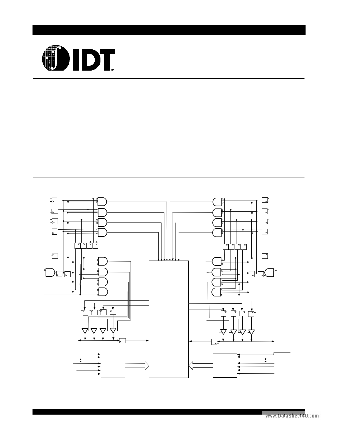
Functional Block Diagram
BE3L
BE2L
BE1L
BE0L
address inputs @ 133MHz
– Data input, address, byte enable and control registers
– Self-timed write allows fast cycle time
x Separate byte controls for multiplexed bus and bus
matching compatibility
x LVTTL- compatible, single 3.3V (±150mV) power supply for
core
x LVTTL compatible, selectable 3.3V (±150mV)/2.5V (±125mV)
power supply for I/Os and control signals on each port
x Industrial temperature range (-40°C to +85°C) is
available for selected speeds
x Available in a 208-pin Plastic Quad Flatpack (PQFP) and
208-pin fine pitch Ball Grid Array, and 256-pin Ball Grid
Array
BE3R
BE2R
BE1R
BE0R
R/WL
CE0L
CE1L
OEL
I/O0L- I/O35L
CLKL
A14L
A0L
CNTRSTL
ADSL
CNTENL
Counter/
Address
Reg.
B B B B B BB B
W W W W W WW W
0 1 2 3 3 21 0
L L L L R RR R
Dout0-8_L
Dout9-17_L
Dout18-26_L
Dout27-35_L
Dout0-8_R
Dout9-17_R
Dout18-26_R
Dout27-35_R
32K x 36
MEMORY
ARRAY
Din_L
Din_R
ADDR_L
ADDR_R
Counter/
Address
Reg.
©2001 Integrated Device Technology, Inc.
1
R/WR
CE0R
CE1R
OER
I/O0R - I/O35R
A14R
CLKR
A0R
CNTRSTR
ADSR
CNTENR
,
4830 tbl 01
JULY 2001
DSC 4830/13
1 page 
IDT70V3579S
High-Speed 32K x 36 Dual-Port Synchronous Pipelined Static RAM
Industrial and Commercial Temperature Ranges
Pin Names
www.DLeafttaPSohrteet4U.comRight Port
Names
CE0L, CE1L
R/WL
CE0R, CE1R
R/WR
Chip Enables
Read/Write Enable
OEL OER Output Enable
A0L - A14L
A0R - A14R
Address
I/O0L - I/O35L
I/O0R - I/O35R
Data Input/Output
CLKL
CLKR
Clock
ADSL
CNTENL
CNTRSTL
BE0L - BE3L
VDDQL
OPTL
ADSR
CNTENR
CNTRSTR
BE0R - BE3R
VDDQR
OPTR
VDD
VSS
Address Strobe Enable
Counter Enable
Counter Reset
Byte Enables (9-bit bytes)
Power (I/O Bus) (3.3V or 2.5V)(1)
Option for selecting VDDQX(1,2)
Power (3.3V)(1)
Ground (0V)
4830 tbl 01
NOTES:
1. VDD, OPTX, and VDDQX must be set to appropriate operating levels prior to
applying inputs on the I/Os and controls for that port.
2. OPTX selects the operating voltage levels on that port. If OPTX is set to VIH (3.3V),
then that port's I/Os and controls will operate at 3.3V levels and VDDQX must be
supplied at 3.3V. If OPTX is set to VIL (0V), then that port's I/Os and controls will
operate at 2.5V levels and VDDQX must be supplied at 2.5V. The OPT pins are
independent of one another—both ports can operate at 3.3V levels, both can
operate at 2.5V levels, or either can operate at 3.3V with the other at 2.5V.
Truth Table IRead/Write and Enable Control(1,2,3,4)
Byte 3
OE CLK CE0 CE1 BE3 BE2 BE1 BE0 R/W I/O27-35
Byte 2
I/O18-2 6
Byte 1
I/O9-17
Byte 0
I/O0-8
MODE
X ↑ H X X X X X X High-Z High-Z High-Z High-Z Deselected–Power Down
X ↑ X L X X X X X High-Z High-Z High-Z High-Z Deselected–Power Down
X ↑ L H H H H H X High-Z High-Z High-Z High-Z All Bytes Deselected
X ↑ L H H H H L L High-Z High-Z High-Z
DIN Write to Byte 0 Only
X ↑ L H H H L H L High-Z High-Z DIN High-Z Write to Byte 1 Only
X ↑ L H H L H H L High-Z DIN High-Z High-Z Write to Byte 2 Only
X ↑ L H L H H H L DIN High-Z High-Z High-Z Write to Byte 3 Only
X ↑ L H H H L L L High-Z High-Z
DIN
DIN Write to Lower 2 Bytes Only
X↑L HL L HHL
DIN
DIN High-Z High-Z Write to Upper 2 bytes Only
X↑L HL L L L L
DIN
DIN
DIN
DIN Write to All Bytes
L ↑ L H H H H L H High-Z High-Z High-Z DOUT Read Byte 0 Only
L ↑ L H H H L H H High-Z High-Z DOUT High-Z Read Byte 1 Only
L ↑ L H H L H H H High-Z DOUT High-Z High-Z Read Byte 2 Only
L ↑ L H L H H H H DOUT High-Z High-Z High-Z Read Byte 3 Only
L ↑ L H H H L L H High-Z High-Z DOUT
DOUT Read Lower 2 Bytes Only
L ↑ L H L L H H H DOUT
DOUT High-Z High-Z Read Upper 2 Bytes Only
L ↑ L H L L L L H DOUT
DOUT
DOUT
DOUT Read All Bytes
H ↑ L H L L L L X High-Z High-Z High-Z High-Z Outputs Disabled
NOTES:
1. "H" = VIH, "L" = VIL, "X" = Don't Care.
2. ADS, CNTEN, CNTRST = VIH.
3. OE is an asynchronous input signal.
4. It is possible to read or write any combination of bytes during a given access. A few representative samples have been illustrated here.
65.42
4830 tbl 02
5 Page 
IDT70V3579S
High-Speed 32K x 36 Dual-Port Synchronous Pipelined Static RAM
Industrial and Commercial Temperature Ranges
Timing Waveform of Read Cycle for Pipelined Operation(2)
www.DataSheet4U.com
tCH2
tCYC2
tCL2
CLK
CE0
CE1
BE(0-3)
tSC tHC
tSB tHB
tSB tHB
(5)
tSC tHC
(3)
R/W
ADDRESS(4)
tSW tHW
tSA tHA
An
An + 1
An + 2
An + 3
DATAOUT
(1 Latency)
tCKLZ (1)
tCD2
tDC
Qn
Qn + 1
tOHZ
tOLZ
Qn + 2 (5)
(1)
OE
tOE
NOTES:
1. OE is asynchronously controlled; all other inputs are synchronous to the rising clock edge.
4830 drw 06
2. ADS = VIL, CNTEN and CNTRST = VIH.
3. The output is disabled (High-Impedance state) by CE0 = VIH, CE1 = VIL, BEn = VIH following the next rising edge of the clock. Refer to Truth Table 1.
4. Addresses do not have to be accessed sequentially since ADS = VIL constantly loads the address on the rising edge of the CLK; numbers
are for reference use only.
5. If BEn was HIGH, then the appropriate Byte of DATAOUT for Qn + 2 would be disabled (High-Impedance state).
Timing Waveform of a Multi-Device Pipelined Read(1,2)
tCYC2
tCH2
tCL2
CLK
tSA tHA
ADDRESS(B1)
A0
A1
A2
A3
A4
CE0(B1)
tSC tHC
tSC tHC
DATAOUT(B1)
ADDRESS(B2)
tSA tHA
A0
tCD2
A1
tCD2
Q0
tDC
A2
tCKHZ
Q1
tDC
A3
tCD2
tCKLZ
A4
A5
Q3
tCKHZ
A5
A6
A6
CE0(B2)
tSC tHC
tSC tHC
tCD2
tCKHZ
DATAOUT(B2)
tCKLZ
Q2
NOTES:
1. B1 Represents Device #1; B2 Represents Device #2. Each Device consists of one IDT70V3579 for this waveform,
and are setup for depth expansion in this example. ADDRESS(B1) = ADDRESS(B2) in this situation.
2. BEn, OE, and ADS = VIL; CE1(B1), CE1(B2), R/W, CNTEN, and CNTRST = VIH.
61.142
tCD2
tCKLZ
Q4
4830 drw 07
11 Page | ||
| Páginas | Total 16 Páginas | |
| PDF Descargar | [ Datasheet IDT70V3579S.PDF ] | |
Hoja de datos destacado
| Número de pieza | Descripción | Fabricantes |
| IDT70V3579S | HIGH-SPEED 3.3V 32K x 36 SYNCHRONOUS PIPELINED DUAL-PORT STATIC RAM | Integrated Device Technology |
| Número de pieza | Descripción | Fabricantes |
| SLA6805M | High Voltage 3 phase Motor Driver IC. |
Sanken |
| SDC1742 | 12- and 14-Bit Hybrid Synchro / Resolver-to-Digital Converters. |
Analog Devices |
|
DataSheet.es es una pagina web que funciona como un repositorio de manuales o hoja de datos de muchos de los productos más populares, |
| DataSheet.es | 2020 | Privacy Policy | Contacto | Buscar |