|
|
|
PDF DS1845 Data sheet ( Hoja de datos )
| Número de pieza | DS1845 | |
| Descripción | Dual NV Potentiometer and Memory | |
| Fabricantes | Dallas Semiconductor | |
| Logotipo | ||
Hay una vista previa y un enlace de descarga de DS1845 (archivo pdf) en la parte inferior de esta página. Total 13 Páginas | ||
|
No Preview Available !
www.DataSheet4U.com
DS1845
Dual NV Potentiometer and Memory
www.dalsemi.com
FEATURES
Two linear taper potentiometers
− DS1845-010 one 10k, 100 position &
one 10k, 256 position
− DS1845-050 one 10k, 100 position &
one 50k, 256 postition
− DS1845-100 one 10k, 100 position &
one 100k, 256 position
256 bytes of EEPROM memory
Access to data and potentiometer control via
a 2-wire interface
External Write Enable pin to protect data and
potentiometer settings
Nonvolatile wiper storage in 2 bytes of
address space
Operates from 3V or 5V supplies
Packaging: Flip Chip Package, 16-ball
STPBGA, 14-pin TSSOP
Industrial operating temperature: -40ºC to
+85ºC
Programming temperature: 0ºC to +70ºC
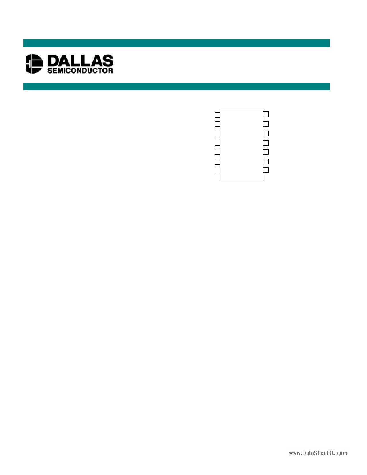
PIN ASSIGNMENT
SDA
SCL
A0
A1
A2
WP
GND
1
2
3
4
5
6
7
14 Vcc
13 H0
12 W1
11 H1
10 L1
9 W0
8 L0
14-Pin TSSOP (173 mil)
14-Pin Flip Chip (100 x 100 mils)
16-BALL STPBGA (4 x 4 mm)
See Mech. Drawing Section
PIN DESCRIPTION
VCC
GND
- 3V or 5V Power Supply Input
- Ground
SDA
- 2-wire Serial Data
Input/Output
SCL - 2-wire Serial Clock Input
WP - Write Protect Input
A0, A1, A2 - Address Inputs
H0, H1
- High-End of Potentiometer
L 0, L1
- Low-End of Potentiometer
W0, W1
- Wiper Terminal of
Potentiometer
DESCRIPTION
The DS1845 Dual NV Potentiometer and Memory consists of one=100-position linear taper
potentiometer, one=256-position linear taper potentiometer, 256 bytes of EEPROM memory, and a 2-wire
interface. The device provides an ideal method for setting bias voltages and currents in control
applications using a minimum of circuitry. The EEPROM memory allows a user to store configuration
or calibration data for a specific system or device as well as provide control of the potentiometer wiper
settings. Any type of user information may reside in the first 248 bytes of this memory. The next two
addresses of EEPROM memory are for potentiometer settings and the remaining 6 bytes of memory are
reserved. These reserved and potentiometer registers should not be used for data storage. Access to this
EEPROM is via an industry standard 2-wire bus. The interface I/O pins consist of SDA and SCL. The
wiper position of the DS1845, as well as EEPROM data, can be hardware write-protected using the Write
Protect (WP) input pin.
1 of 13
051900
1 page 
DS1845
RANDOM READ
A random read requires a dummy byte write sequence to load in the data word address. Once the device
andwwdwa.tDaataadSdhereets4sU.bcoymtes are clocked in by the master, and acknowledged by the DS1845, the master must
generate another start condition. The master now initiates a current address read by sending the device
address with the read/write bit set high. The DS1845 will acknowledge the device address and serially
clocks out the data byte.
SEQUENTIAL ADDRESS READ
Sequential reads are initiated by either a current address read or a random address read. After the master
receives the first data byte, the master responds with an acknowledge. As long as the DS1845 receives
this acknowledge after a byte is read, the master may clock out additional data words from the DS1845.
After reaching address FFh, it resets to address 00h.
The sequential read operation is terminated when the master initiates a stop condition. The master does
not respond with a zero.
For a more detailed description of 2-wire theory of operation, refer to the following section.
2-WIRE SERIAL PORT OPERATION
The 2-wire serial port interface supports a bi-directional data transmission protocol with device
addressing. A device that sends data on the bus is defined as a transmitter, and a device receiving data as
a receiver. The device that controls the message is called a “master.” The devices that are controlled by
the master are “slaves.” The bus must be controlled by a master device that generates the serial clock
(SCL), controls the bus access, and generates the START and STOP conditions. The DS1845 operates as
a slave on the two-wire bus. Connections to the bus are made via the open-drain I/O lines SDA and SCL.
The following I/O terminals control the 2-wire serial port: SDA, SCL, A0, A1, A2. Timing diagrams for
the 2-wire serial port can be found in Figures 2 and 3. Timing information for the 2-wire serial port is
provided in the AC Electrical Characteristics table for 2-wire serial communications.
The following bus protocol has been defined:
- Data transfer may be initiated only when the bus is not busy.
- During data transfer, the data line must remain stable whenever the clock line is HIGH. Changes in
the data line while the clock line is HIGH will be interpreted as control signals.
Accordingly, the following bus conditions have been defined:
Bus not busy: Both data and clock lines remain HIGH.
Start data transfer: A change in the state of the data line from HIGH to LOW while the clock is HIGH
defines a START condition.
Stop data transfer: A change in the state of the data line from LOW to HIGH while the clock line is
HIGH defines the STOP condition.
5 of 13
5 Page 
AC ELECTRICAL CHARACTERISTICS
PARAMETER
www.DataSheet4U.com
SCL clock frequency
SYMBOL CONDITION
fSCL
Bus free time between
STOP and START
condition
Hold time (repeated)
START condition
Low period of SCL clock
tBUF
tHD:STA
tLOW
High period of SCL clock tHIGH
Data hold time
tHD:DAT
Data set-up time
tSU:DAT
Start set-up time
tSU:STA
Rise time of both SDA
and SCL signals
Fall time of both SDA
and SCL signals
Set-up time for STOP
condition
Capacitive load for each
bus line
EEPROM write time
* fast mode
** standard mode
tR
tF
tSU:STO
CB
TW
DS1845
(-40oC to 85oC, Vcc=2.7V to 5.5V)
MIN TYP MAX UNITS NOTES
0
400 kHz
*,6
0 100
**
1.3 µs *,6
4.7 **
0.6
4.0
1.3
4.7
0.6
4.0
0
0
100
250
0.6
4.7
20+0.1
CB
20+0.1
CB
0.6
4.0
0.9
300
1000
300
300
400
µs
µs
µs
µs
ns
µs
ns
ns
µs
pF
*,7,6
**
*,6
**
*,6
**
*,6,8
**
*,6
**
*,6
**
*,9
**
*,9
**
*
**
9
5 ms 10
NOTES:
1. All voltages are referenced to ground.
2. ISTBY specified with for VCC equal 3.0V and 5.0V and control port logic pins are driven to the
appropriate logic levels. Appropriate logic levels specify that logic inputs are within a 0.5V of
ground or VCC for the corresponding inactive state.
3. I/O pins of fast mode devices must not obstruct the SDA and SCL lines if VCC is switched off.
4. Address Inputs, A0, A1, and A2, should be tied to either VCC or GND depending on the desired
address selections.
5. ISTBY specified with for VCC equal 3.0V and 5.0V and control port logic pins are driven to the
appropriate logic levels. Appropriate logic levels specify that logic inputs are within a 0.5V of
ground or VCC for the corresponding inactive state.
11 of 13
11 Page | ||
| Páginas | Total 13 Páginas | |
| PDF Descargar | [ Datasheet DS1845.PDF ] | |
Hoja de datos destacado
| Número de pieza | Descripción | Fabricantes |
| DS1841 | Temperature-Controlled | Maxim Integrated Products |
| DS1842 | Bias Output Stage | Maxim Integrated Products |
| DS1842A | Bias Output Stage | Maxim Integrated Products |
| DS1843 | RSSI Burst-Mode Sample-and-Hold Circuit | Maxim Integrated Products |
| Número de pieza | Descripción | Fabricantes |
| SLA6805M | High Voltage 3 phase Motor Driver IC. |
Sanken |
| SDC1742 | 12- and 14-Bit Hybrid Synchro / Resolver-to-Digital Converters. |
Analog Devices |
|
DataSheet.es es una pagina web que funciona como un repositorio de manuales o hoja de datos de muchos de los productos más populares, |
| DataSheet.es | 2020 | Privacy Policy | Contacto | Buscar |