|
|
|
PDF IDT72V3646 Data sheet ( Hoja de datos )
| Número de pieza | IDT72V3646 | |
| Descripción | (IDT72V36x6) 3.3 VOLT CMOS TRIPLE BUS SyncFIFO | |
| Fabricantes | Integrated Device Technology | |
| Logotipo | ||
Hay una vista previa y un enlace de descarga de IDT72V3646 (archivo pdf) en la parte inferior de esta página. Total 36 Páginas | ||
|
No Preview Available !
www.DataSheet4U.com
3.3 VOLT CMOS TRIPLE BUS
SyncFIFOTM WITH BUS-MATCHING
256 x 36 x 2, 512 x 36 x 2,
1,024 x 36 x 2
IDT72V3626
IDT72V3636
IDT72V3646
.EATURES:
• Memory storage capacity:
IDT72V3626–256 x 36 x 2
IDT72V3636–512 x 36 x 2
IDT72V3646–1,024 x 36 x 2
• Clock frequencies up to 100 MHz (6.5ns access time)
• Two independent FIFOs buffer data between one bidirectional
36-bit port and two unidirectional 18-bit ports (Port C receives
and Port B transmits)
• 18-bit (word) and 9-bit (byte) bus sizing of 18 bits (word) on
Ports B and C
• Select IDT Standard timing (using EFA, EFB, FFA, and FFC flag
functions) or First Word Fall Through Timing (using ORA, ORB,
IRA, and IRC flag functions)
• Programmable Almost-Empty and Almost-Full flags; each has
three default offsets (8, 16 and 64)
• Serial or parallel programming of partial flags
• Big- or Little-Endian format for word and byte bus sizes
• Master Reset clears data and configures FIFO, Partial Reset
clears data but retains configuration settings
• Mailbox bypass registers for each FIFO
• Free-running CLKA, CLKB and CLKC may be asynchronous or
coincident (simultaneous reading and writing of data on a single
clock edge is permitted)
• Auto power down minimizes power dissipation
• Available in a space-saving 128-pin Thin Quad Flatpack (TQFP)
• Pin and functionally compatible versions of 5V operating
IDT723626/723636/723646
• Industrial temperature range (–40°C to +85°C) is available
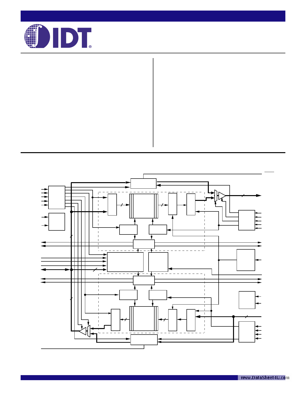
.UNCTIONAL BLOCK DIAGRAM
CLKA
CSA
W/RA
ENA
MBA
MRS1
PRS1
FFA/IRA
AFA
SPM
FS0/SD
FS1/SEN
A0-A35
EFA/ORA
AEA
Port-A
Control
Logic
FIFO1,
Mail1
Reset
Logic
36
36
MBF2
Mail 1
Register
36
RAM ARRAY
256 x 36
36
512 x 36
1,024 x 36
FIFO1
Write
Pointer
Read
Pointer
Status Flag
Logic
Programmable Flag
Offset Registers
Timing
Mode
10
FIFO2
Status Flag
Logic
Read
Pointer
Write
Pointer
RAM ARRAY
36 256 x 36
512 x 36
1,024 x 36
36
Mail 2
Register
MBF1
18
B0-B17
Port-B
Control
Logic
CLKB
RENB
CSB
MBB
SIZEB
Common
Port
Control
Logic
(B and C)
EFB/ORB
AEB
BE
FWFT
FFC/IRC
AFC
FIFO2,
Mail2
Reset
Logic
18
Port-C
Control
Logic
MRS2
PRS2
C0-C17
CLKC
WENC
MBC
SIZEC
4665 drw01
IDT, the IDT logo are registered trademarks of Integrated Device Technology, Inc. SyncFIFO is a trademark of Integrated Device Technology, Inc.
COMMERCIAL TEMPERATURE RANGE
1
2001 Integrated Device Technology, Inc. All right reserved. Product specifications subject to change without notice.
AUGUST 2001
DSC-4665/4
1 page 
IDIDTT7722VV33662266//7722VV3363663/67/27V23V634664C6MCOMSO3S.33V.3TVriTpRleIPBLuEs BSyUnScFSIyFnOcTMFIFOTM
WwIiTthHBBuUsS-M-MatAchTiCngHI2N5G6x2365x62x, 53162x326,x521, 21,x02346x3x62x,21,024 x 36 x 2
COMMERCIALTEMPERATURERANGE
PIN DESCRIPTIONS (Continued)
Symbol
Name
I/O
Description
FS1w/SwEwN.DaFtalaSghOeeffst4eUt S.ceolemct 1/
Serial Enable,
I FS1/SEN and FS0/SD are dual-purpose inputs used for flag Offset register programming. During Master Reset,
FS1/SEN and FS0/SD, together with SPM, select the flag offset programming method. Three Offset register
programming methods are available: automatically load one of three preset values (8, 16, or 64), parallel
FS0/SD FlagOffsetSelect0/
load from Port A, and serial load.
Serial Data
When serial load is selected for flag Offset register programming, FS1/SEN is used as an enable synchronous to
the LOW-to-HIGH transition of CLKA. When FS1/SEN is LOW, a rising edge on CLKA load the bit present on
FS0/SD into the X and Y registers. The number of bit writes required to program the Offset registers is 32 for the
72V3626, 36 for the 72V3636, and 40 for the 72V3646. The first bit write stores the Y-register (Y1) MSB and the
last bit write stores the X-register (X2) LSB.
MBA Port A Mailbox
Select
I A HIGH level on MBA chooses a mailbox register for a Port A read or write operation. When the A0-A35
outputs are active, a HIGH level on MBA selects data from the mail2 register for output and a LOW level selects
FIFO2 output-register data for output.
MBB Port B Mailbox
Select
I A HIGH level on MBB chooses a mailbox register for a Port B read operation. When the B0-B17 outputs are
active, a HIGH level on MBB selects data from the mail1 register for output and a LOW level selects FIFO1 output
register data for output.
MBC
MBF1
Port C Mailbox
Select
Mail1 Register
Flag
MBF2
Mail2 Register
Flag
MRS1 Master Reset
MRS2 Master Reset
PRS1 PartialReset
PRS2 PartialReset
I A HIGH level on MBC chooses the mail2 register for a Port C write operation. This pin must be HIGH during
Master Reset.
O MBF1 is set LOW by a LOW-to-HIGH transition of CLKA that writes data to the mail1 register. Writes to the mail1
register are inhibited while MBF1 is LOW. MBF1 is set HIGH by a LOW-to-HIGH transition of CLKB when a
Port B read is selected and MBB is HIGH. MBF1 is set HIGH following either a Master or Partial Reset of FIFO1.
O MBF2 is set LOW by a LOW-to-HIGH transition of CLKC that writes data to the mail2 register. Writes to the mail2
register are inhibited while MBF2 is LOW. MBF2 is set HIGH by a LOW-to-HIGH transition of CLKA when a
Port A read is selected and MBA is HIGH. MBF2 is set HIGH following either a Master or Partial Reset of FIFO2.
I A LOW on this pin initializes the FIFO1 read and write pointers to the first location of memory and sets the Port B
output register to all zeroes. A LOW-to-HIGH transition on MRS1 selects the programming method (serial or
parallel) and one of three programmable flag default offsets for FIFO1 and FIFO2. It also configures ports B and
C for bus size and endian arrangement. Four LOW-to-HIGH transitions of CLKA and four LOW-to-HIGH
transitions of CLKB must occur while MRS1 is LOW.
I A LOW on this pin initializes the FIFO2 read and write pointers to the first location of memory and sets the Port A
output register to all zeroes. A LOW-to-HIGH transition on MRS2, toggled simultaneously with MRS1, selects
the programming method (serial or parallel) and one of the three flag default offsets for FIFO2. Four LOW-to-HIGH
transitions of CLKA and four LOW-to-HIGH transitions of CLKC must occur while MRS2 is LOW.
I A LOW on this pin initializes the FIFO1 read and write pointers to the first location of memory and sets thePort B
output register to all zeroes. During Partial Reset, the currently selected bus size, endian arrangement,
programming method (serial or parallel), and programmable flag settings are all retained.
I A LOW on this pin initializes the FIFO2 read and write pointers to the first location of memory and sets thePort A
output register to all zeroes. During Partial Reset, the currently selected bus size, endian arrangement,
programming method (serial or parallel), and programmable flag settings are all retained.
RENB Port B Read Enable I RENB must be HIGH to enable a LOW-to-HIGH transition of CLKB to read data on Port B.
SIZEB Port B
Bus Size Select
I SIZEB determines the bus width of Port B. A HIGH on this pin selects byte (9-bit) bus size. A LOW on this pin
selects word (18-bit) bus size. SIZEB works with SIZEC and BE to select the bus size and endian arrangement
for ports B and C. The level of SIZEB must be static throughout device operation.
SIZEC
SPM
Port C
Bus Size Select
Serial Programming
Mode
I SIZEC determines the bus width of Port C. A HIGH on this pin selects byte (9-bit) bus size. A LOW on this pin
selects word (18-bit) bus size. SIZEC works with SIZEB and BE to select the bus size and endian arrangement
for ports B and C. The level of SIZEC must be static throughout device operation.
I A LOW on this pin selects serial programming of partial flag offsets. A HIGH on this pin selects parallel
programming or default offsets (8, 16, or 64).
WENC
W/RA
Port C Write Enable
Port A Write/
Read Select
I WENC must be HIGH to enable a LOW-to-HIGH transition of CLKC to write data on Port C.
I A HIGH selects a write operation and a LOW selects a read operation on Port A for a LOW-to-HIGH transition of
CLKA. The A0-A35 outputs are in the HIGH impedance state when W/RA is HIGH.
5
5 Page 
IDIDTT7722VV33662266//7722VV3363663/67/27V23V634664C6MCOMSO3S.33V.3TVriTpRleIPBLuEs BSyUnScFSIyFnOcTMFIFOTM
WwIiTthHBBuUsS-M-MatAchTiCngHI2N5G6x2365x62x, 53162x326,x521, 21,x02346x3x62x,21,024 x 36 x 2
COMMERCIALTEMPERATURERANGE
FollowingMasterReset,thelevelappliedtotheBE/FWFT inputtochoose
thedesiredtimingmodemustremainstaticthroughoutFIFOoperation. Refer
to Figure 4 (FIFO1 Master Reset) and Figure 5 (FIFO2 Master Reset) for First
WordwFwawll.TDhartoauSghheseet4leUct.ctiomming diagrams.
PROGRAMMING THE ALMOST-EMPTY AND ALMOST-FULL FLAGS
FourregistersintheseFIFOsareusedtoholdtheoffsetvaluesfortheAlmost-
Empty and Almost-Full flags. The Port B Almost-Empty flag (AEB) Offset register
is labeled X1 and the Port A Almost-Empty flag (AEA) Offset register is labeled
X2. The Port A Almost-Full flag (AFA) Offset register is labeled Y1 and the Port
C Almost-Full flag (AFC) Offset register is labeled Y2. The index of each register
name corresponds to its FIFO number. The Offset registers can be loaded with
preset values during the reset of a FIFO, programmed in parallel using the
FIFO’s Port A data inputs, or programmed in serial using the Serial Data (SD)
input (see Table 1).
SPM, FS0/SD, and FS1/SENfunction the same way in both IDT Standard
and FWFT modes.
— PRESET VALUES
To load a FIFO’s Almost-Empty flag and Almost-Full flag Offset registers with
one of the three preset values listed in Table 1, the Serial Program Mode (SPM)
and at least one of the flag select inputs must be HIGH during the LOW-to-HIGH
transitionofitsMasterReset(MRS1and MRS2)input.Forexample,toloadthe
preset value of 64 into X1 and Y1, SPM, FS0 and FS1 must be HIGH when FlFO1
reset (MRS1) returns HIGH. Flag Offset registers associated with FIFO2 are
loaded with one of the preset values in the same way with FIFO2 Master Reset
(MRS2) toggled simultaneously with FIFO1 Master Reset (MRS1). For relevant
Preset value loading timing diagrams, see Figure 4 and 5.
— PARALLEL LOAD FROM PORT A
To program the X1, X2, Y1, and Y2 registers from Port A, perform a Master
Reset on both FlFOs simultaneously with SPMHIGH and FS0 and FS1 LOW
during the LOW-to-HIGH transition of MRS1 and MRS2. After this reset is
complete,thefirstfourwritestoFIFO1donotstoredatainRAMbutloadtheOffset
registers in the order Y1, X1, Y2, X2. The Port A data inputs used by the Offset
registers are (A7-A0), (A8-A0), or (A9-A0) for the IDT72V3626, IDT72V3636,
or IDT72V3646, respectively. The highest numbered input is used as the most
significant bit of the binary number in each case. Valid programming values for
the registers range from 1 to 252 for the IDT72V3626; 1 to 508 for the
IDT72V3636; and 1 to 1,020 for the IDT72V3646. After all the Offset registers
are programmed from Port A, the Port C Full/Input Ready flag (FFC/IRC) is
set HIGH, and both FIFOs begin normal operation. Refer to Figure 8 for a timing
diagram illustration for parallel programming of the flag offset values.
— SERIAL LOAD
To program the X1, X2, Y1, and Y2 registers serially, initiate a Master Reset
with SPMLOW, FS0/SD LOW and FS1/SEN HIGH during the LOW-to-HIGH
transitionof MRS1andMRS2.Afterthisresetiscomplete,theXandYregister
values are loaded bit-wise through the FS0/SD input on each LOW-to-HIGH
transition of CLKA that the FS1/SEN input is LOW. There are 32-, 36-, or 40-
bitwritesneededtocompletetheprogrammingfortheIDT72V3626,IDT72V3636,
or IDT72V3646, respectively. The four registers are written in the order Y1,
X1, Y2 and finally, X2. The first-bit write stores the most significant bit of the Y1
registerandthelast-bitwritestorestheleastsignificantbitoftheX2register.Each
register value can be programmed from 1 to 252 (IDT72V3626), 1 to 508
(IDT72V3636), or 1 to 1,020 (IDT72V3646).
When the option to program the Offset registers serially is chosen, the Port
A Full/Input Ready (FFA/IRA) flag remains LOW until all register bits are written.
FFA/IRA is set HIGH by the LOW-to-HIGH transition of CLKA after the last bit
is loaded to allow normal FIFO1 operation. The Port B Full/Input Ready (FFC/
IRC) flag also remains LOW throughout the serial programming process, until
all register bits are written. FFC/IRC is set HIGH by the LOW-to-HIGH transition
of CLKC after the last bit is loaded to allow normal FIFO2 operation.
See Figure 9 timing diagram, Serial Programming of the Almost-Full Flag
and Almost-Empty Flag Offset Values after Reset (IDT Standard and FWFT
Modes).
FIFO WRITE/READ OPERATION
The state of the Port A data (A0-A35) outputs is controlled by Port A Chip
Select (CSA) and Port A Write/Read Select (W/RA). The A0-A35 outputs are
in the high-impedance state when either CSA or W/RA is HIGH. The A0-A35
outputs are active when both CSA and W/RA are LOW.
Data is loaded into FIFO1 from the A0-A35 inputs on a LOW-to-HIGH
transition of CLKA when CSA is LOW, W/RA is HIGH, ENA is HIGH, MBA is
TABLE 1 .LAG PROGRAMMING
SPM FS1/SEN FS0/SD MRS1 MRS2
H H H ↑X
H H H ↑↑
H H L ↑X
H H L ↑↑
H L H ↑X
H L H ↑↑
H L L ↑↑
L H L ↑↑
L H H ↑↑
L L H ↑↑
L L L ↑↑
NOTES:
1. X1 register holds the offset for AEB; Y1 register holds the offset for AFA.
2. X2 register holds the offset for AEA; Y2 register holds the offset for AFC.
X1 AND Y1 REGlSTERS(1)
64
64
16
16
8
8
Parallel programming via Port A
Serial programming via SD
Reserved
Reserved
Reserved
11
X2 AND Y2 REGlSTERS(2)
X
64
X
16
X
8
Parallel programming via Port A
Serial programming via SD
Reserved
Reserved
Reserved
11 Page | ||
| Páginas | Total 36 Páginas | |
| PDF Descargar | [ Datasheet IDT72V3646.PDF ] | |
Hoja de datos destacado
| Número de pieza | Descripción | Fabricantes |
| IDT72V3640 | 3.3 VOLT HIGH-DENSITY SUPERSYNC II 36-BIT FIFO | Integrated Device Tech |
| IDT72V3641 | (IDT72V36x1) 3.3 VOLT CMOS SyncFIFOTM | Integrated Device Technology |
| IDT72V3642 | 3.3 VOLT CMOS SyncBiFIFO 256 x 36 x 2 512 x 36 x 2 1/024 x 36 x 2 | Integrated Device Tech |
| IDT72V3643 | (IDT72V36x3) 3.3 VOLT CMOS SyncFIFO | Integrated Device Technology |
| Número de pieza | Descripción | Fabricantes |
| SLA6805M | High Voltage 3 phase Motor Driver IC. |
Sanken |
| SDC1742 | 12- and 14-Bit Hybrid Synchro / Resolver-to-Digital Converters. |
Analog Devices |
|
DataSheet.es es una pagina web que funciona como un repositorio de manuales o hoja de datos de muchos de los productos más populares, |
| DataSheet.es | 2020 | Privacy Policy | Contacto | Buscar |