|
|
|
PDF ICS83940D Data sheet ( Hoja de datos )
| Número de pieza | ICS83940D | |
| Descripción | 1-TO-18 LVPECL-TO-LVCMOS / LVTTL FANOUT BUFFER | |
| Fabricantes | Integrated Circuit Systems | |
| Logotipo | ||
Hay una vista previa y un enlace de descarga de ICS83940D (archivo pdf) en la parte inferior de esta página. Total 15 Páginas | ||
|
No Preview Available !
Integrated
Circuit
Systems, Inc.
ICS83940D
LOW SKEW, 1-TO-18
LVPECL-TO-LVCMOS / LVTTL FANOUT BUFFER
GENERAL DESCRIPTION
The ICS83940D is a low skew, 1-to-18 LVPECL-
ICS to-LVCMOS/LVTTL Fanout Buffer and a member
HiPerClockS™ of the HiPerClockS™family of High Performance
Clock Solutions from ICS. The ICS83940D has
two selectable clock inputs. The PCLK, nPCLK
pair can accept LVPECL, CML, or SSTL input levels. The
LVCMOS_CLK can accept LVCMOS or LVTTL input levels.
The low impedance LVCMOS/LVTTL outputs are designed to
www.DataSheedt4riUve.co5m0Ω series or parallel terminated transmission lines.
The ICS83940D is characterized at full 3.3V and 2.5V or mixed
3.3V core, 2.5V output operating supply modes. Guaranteed
output and part-to-part skew characteristics make the
ICS83940D ideal for those clock distribution applications
demanding well defined performance and repeatability.
FEATURES
• 18 LVCMOS/LVTTL outputs
• Selectable LVCMOS_CLK or LVPECL clock inputs
• PCLK, nPCLK supports the following input types:
LVPECL, CML, SSTL
• LVCMOS_CLK accepts the following input levels:
LVCMOS or LVTTL
• Maximum output frequency: 250MHz
• Output skew: 150ps (maximum)
• Part to part skew: 750ps (maximum)
• Additive phase jitter, RMS: < 0.03ps (typical)
• Full 3.3V and 2.5V or mixed 3.3V core, 2.5V output
supply modes
• 0°C to 70°C ambient operating temperature
• Lead-Free package available
• Pin compatible with the MPC940L
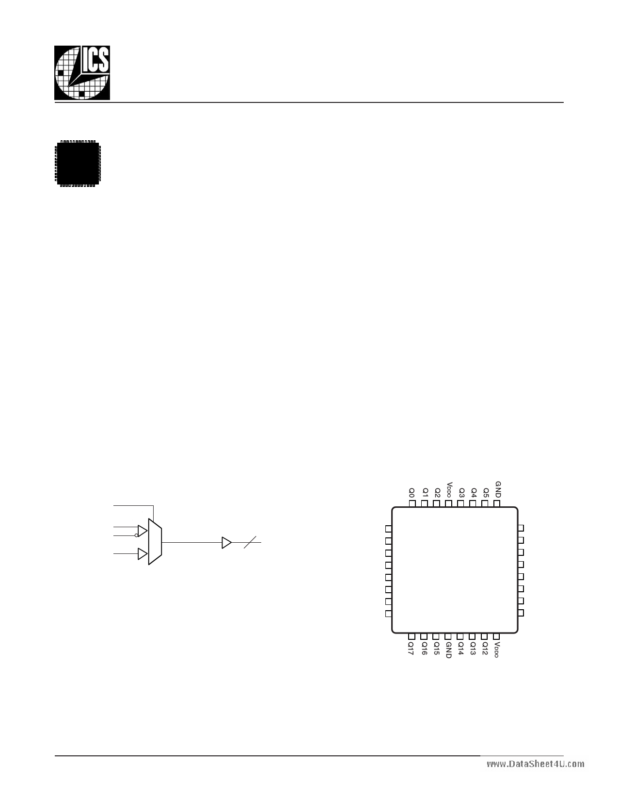
BLOCK DIAGRAM
CLK_SEL
PCLK
nPCLK
LVCMOS_CLK
0
1
83940DY
PIN ASSIGNMENT
18
Q0:Q17
GND
GND
LVCMOS_CLK
CLK_SEL
PCLK
nPCLK
VDD
VDDO
32 31 30 29 28 27 26 25
1 24
2 23
3 22
4 ICS83940D 21
5 20
6 19
7 18
8 17
9 10 11 12 13 14 15 16
Q6
Q7
Q8
VDD
Q9
Q10
Q11
GND
32-Lead LQFP
7mm x 7mm x 1.4mm package body
Y Pacakge
Top View
www.icst.com/products/hiperclocks.html
1
REV. B JUNE 15, 2004
1 page 
Integrated
Circuit
Systems, Inc.
ICS83940D
LOW SKEW, 1-TO-18
LVPECL-TO-LVCMOS / LVTTL FANOUT BUFFER
TABLE 4B. DC CHARACTERISTICS, VDD = 3.3V ± 5%, VDDO = 2.5V ± 5%, TA = 0° TO 70°
Symbol Parameter
Test Conditions Minimum Typical
VIH
VIL
VPP
VCMR
Input High Voltage
LVCMOS_CLK
Input Low Voltage
LVCMOS_CLK
Peak-to-Peak Input Voltage PCLK, nPCLK
Input Common Mode Voltage;
NOTE 1, 2
PCLK, nPCLK
2.4
300
VDD - 1.4
www.DataSheet4IIUN .com Input Current
VOH Output High Voltage
IOH = -20mA
1.8
VOL Output Low Voltage
IOL = 20mA
IDD Core Supply Current
NOTE 1: For single ended applications, the maximum input voltage for PCLK, nPCLK is VDD + 0.3V.
NOTE 2: Common mode voltage is defined as VIH.
Maximum
VDD
0.8
1000
VDD - 0.6
±200
0.5
25
Units
V
V
mV
V
µA
V
V
mA
TABLE 5B. AC CHARACTERISTICS, VDD = 3.3V ± 5%, VDDO = 2.5V ± 5%, TA = 0° TO 70°
Symbol Parameter
Test Conditions
Minimum Typical Maximum Units
fMAX
tpLH
t
pLH
tsk(o)
tsk(pp)
Output Frequency
Propagation Delay
Propagation Delay
Output Skew;
NOTE 3, 5
Part-to-Part Skew;
NOTE 6
PCLK, nPCLK;
NOTE 1, 5
LVCMOS_CLK;
NOTE 2, 5
PCLK, nPCLK;
NOTE 1, 5
LVCMOS_CLK;
NOTE 2, 5
PCLK, nPCLK
LVCMOS_CLK
PCLK, nPCLK
LVCMOS_CLK
f ≤ 150MHz
f ≤ 150MHz
f > 150MHz
f > 150MHz
Measured on
rising edge @VDDO/2
f ≤ 150MHz
f ≤ 150MHz
1.7
1.7
1.6
1.8
250 MHz
3.2 ns
3.0 ns
3.4 ns
3.3 ns
150 ps
150 ps
1.5 ns
1.3 ns
tsk(pp)
Part-to-Part Skew;
NOTE 6
PCLK, nPCLK
LVCMOS_CLK
f > 150MHz
f > 150MHz
1.8 ns
1.5 ns
tsk(pp)
tjit
Part-to-Part Skew; PCLK, nPCLK
NOTE 4, 5
LVCMOS_CLK
Buffer Additive Phase Jitter, RMS;
refer to Additive Phase Jitter section,
NOTE 7
Measured on
rising edge @VDDO/2
850 ps
750 ps
0.03 ps
t /t
RF
odc
Output Rise/Fall Time
Output Duty Cycle
0.5 to 1.8V
f < 134MHz
0.3 1.2 ns
45 50 55 %
All parameters measured at 200MHz unless noted otherwise.
NOTE 1: Measured from the differential input crossing point to the output VDDO/2.
NOTE 2: Measured from VDD/2 to VDDO/2.
NOTE 3: Defined as skew between outputs at the same supply voltage and with equal load conditions. Measured at VDDO/2.
NOTE 4: Defined as skew between outputs on different devices operating at the same supply voltages, same temperature,
and with equal load conditions. Using the same type of inputs on each device, the outputs are measured at VDDO/2.
NOTE 5: This parameter is defined in accordance with JEDEC Standard 65.
NOTE 6: Defined as skew between outputs on different devices, across temperature and voltage ranges, and with equal
load conditions. Using the same type of inputs on each device, the outputs are measured at VDDO/2.
NOTE 7: Driving only one input clock.
83940DY
www.icst.com/products/hiperclocks.html
REV. B JUNE 15, 2004
5
5 Page 
Integrated
Circuit
Systems, Inc.
ICS83940D
LOW SKEW, 1-TO-18
LVPECL-TO-LVCMOS / LVTTL FANOUT BUFFER
LVPECL CLOCK INPUT INTERFACE
The PCLK /nPCLK accepts LVPECL, CML, SSTL and other
differential signals. Both VSWING and VOH must meet the VPP
and VCMR input requirements. Figures 2A to 2F show interface
examples for the HiPerClockS PCLK/nPCLK input driven by
the most common driver types. The input interfaces suggested
here are examples only. If the driver is from another vendor,
use their termination recommendation. Please consult with
the vendor of the driver component to confirm the driver ter-
mination requirements.
www.DataSheet4U.com
3.3V
CML
Zo = 50 Ohm
Zo = 50 Ohm
3.3V
R1 R2
50 50
3.3V
PCLK
nPCLK HiPerClockS
PCLK/nPCLK
3.3V
Zo = 50 Ohm
3.3V
R1 PCLK
100
nPCLK
Zo = 50 Ohm
HiPerClockS
CML Built-In Pullup
PCLK/nPCLK
FIGURE 2A. HIPERCLOCKS PCLK/nPCLK INPUT DRIVEN
BY AN OPEN COLLECTOR CML DRIVER
FIGURE 2B. HIPERCLOCKS PCLK/nPCLK INPUT DRIVEN
BY A BUILT-IN PULLUP CML DRIVER
3.3V
Zo = 50 Ohm
LVPEC L
Zo = 50 Ohm
3. 3V
R3 R4
125 125
3.3V
PCLK
nPCLK HiPerClockS
Input
R1 R2
84 84
3.3V
3.3V LVPECL
Zo = 50 Ohm
Zo = 50 Ohm
3.3V
R3 R4
84
C1
84
C2
R5
100 - 200
R6
100 - 200
R1 R2
125 125
3.3V
PCLK
nPCLK HiPerClockS
PCLK/nPCLK
FIGURE 2C. HIPERCLOCKS PCLK/nPCLK INPUT DRIVEN
BY A 3.3V LVPECL DRIVER
FIGURE 2D. HIPERCLOCKS PCLK/nPCLK INPUT DRIVEN
BY A 3.3V LVPECL DRIVER WITH AC COUPLE
2.5V
SSTL
Zo = 60 Ohm
Zo = 60 Ohm
2.5V
R3 R4
120 120
3.3V
PCLK
R1 R2
120 120
nPCLK
HiPerClockS
PCLK/nPCLK
3.3V
LVDS
Zo = 50 Ohm
Zo = 50 Ohm
R5
100
3.3V
3.3V
R3 R4
1K 1K
C1
PCLK
C2
nPCLK
HiPerClockS
PC L K / n PC L K
R1 R2
1K 1K
FIGURE 2E. HIPERCLOCKS PCLK/nPCLK INPUT DRIVEN
BY AN SSTL DRIVER
FIGURE 2F. HIPERCLOCKS PCLK/nPCLK INPUT DRIVEN
BY A 3.3V LVDS DRIVER
83940DY
www.icst.com/products/hiperclocks.html
11
REV. B JUNE 15, 2004
11 Page | ||
| Páginas | Total 15 Páginas | |
| PDF Descargar | [ Datasheet ICS83940D.PDF ] | |
Hoja de datos destacado
| Número de pieza | Descripción | Fabricantes |
| ICS83940 | 1-TO-18 LVCMOS FANOUT BUFFER | Integrated Circuit Systems |
| ICS83940-01 | 1-TO-18 LVCMOS FANOUT BUFFER | Integrated Circuit Systems |
| ICS83940-02 | 1-TO-18 LVCMOS FANOUT BUFFER | Integrated Circuit Systems |
| ICS83940D | 1-TO-18 LVPECL-TO-LVCMOS / LVTTL FANOUT BUFFER | Integrated Circuit Systems |
| Número de pieza | Descripción | Fabricantes |
| SLA6805M | High Voltage 3 phase Motor Driver IC. |
Sanken |
| SDC1742 | 12- and 14-Bit Hybrid Synchro / Resolver-to-Digital Converters. |
Analog Devices |
|
DataSheet.es es una pagina web que funciona como un repositorio de manuales o hoja de datos de muchos de los productos más populares, |
| DataSheet.es | 2020 | Privacy Policy | Contacto | Buscar |