|
|
|
PDF ICS8343-01 Data sheet ( Hoja de datos )
| Número de pieza | ICS8343-01 | |
| Descripción | 1-TO-16 LVCMOS / LVTTL FANOUT BUFFER | |
| Fabricantes | Integrated Circuit Systems | |
| Logotipo | ||
Hay una vista previa y un enlace de descarga de ICS8343-01 (archivo pdf) en la parte inferior de esta página. Total 10 Páginas | ||
|
No Preview Available !
Integrated
Circuit
Systems, Inc.
ICS8343-01
LOW SKEW, 1-TO-16
LVCMOS / LVTTL FANOUT BUFFER
GENERAL DESCRIPTION
ICS
The ICS8343-01 is a low skew, 1-to-16 LVCMOS/
LVTTL Fanout Buffer and a member of the
HiPerClockS™ HiPerClockS™family of High Performance Clock
Solutions from ICS. The ICS8343-01 single ended
clock input accepts LVCMOS or LVTTL input levels.
The ICS8343-01 operates at 3.3V, 2.5V and mixed 3.3V input and
2.5V supply modes over the commercial temperature range.
Guaranteed output and part-to-part skew characteristics make
www.DataSheetth4eU.IcCoSm8343-01 ideal for those clock distribution applications
demanding well defined performance and repeatability.
FEATURES
• 16 LVCMOS/LVTTL outputs
• 1 LVCMOS/LVTTL clock input
• CLK can accept the following input levels: LVCMOS, LVTTL
• Maximum output frequency: 200MHz
• Dual output enable inputs facilitates 1-to-16 or 1-to-8 input
to output modes
• All inputs are 5V tolerant
• Output skew: 250ps (maximum)
• Part-to-part skew: 700ps (maximum)
• Full 3.3V and 2.5V or mixed 3.3V core/2.5V operating supply
• 0°C to 70°C ambient operating temperature
• Lead-Free package available
• Industrial temperature information available upon request
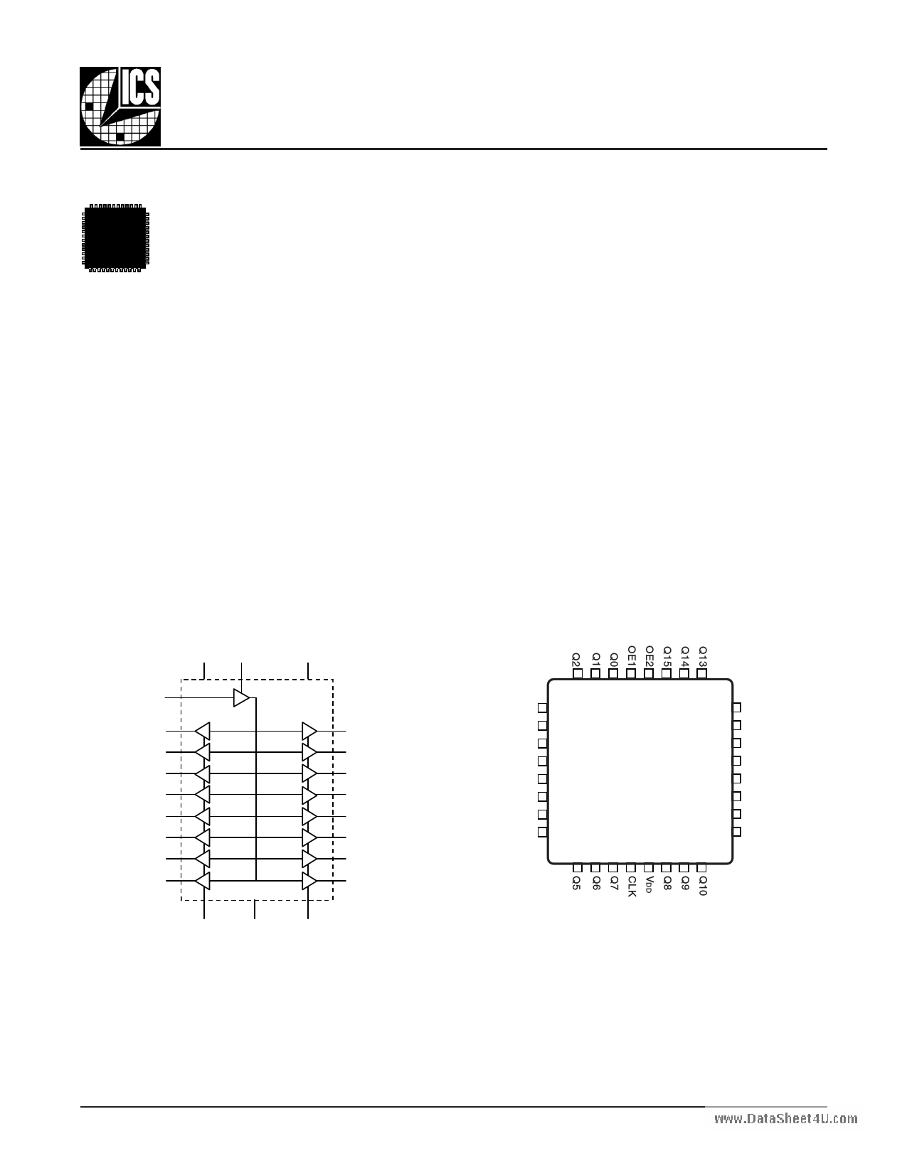
BLOCK DIAGRAM
VVDDDD11 VVDDDD
CCLLKK
QQ00
QQ11
QQ22
QQ33
QQ44
QQ55
QQ66
QQ77
VVDDDD22
QQ155
QQ144
QQ133
QQ122
QQ111
QQ1100
QQ99
QQ8
OOEE11
GGNNDD
OOEE22
PIN ASSIGNMENT
32 31 30 29 28 27 26 25
VDD1
VDD1
VDD1
Q3
Q4
GND
GND
GND
1
2
3
4
5
6
7
8
ICS8343-01
24
23
22
21
20
19
18
17
9 10 11 12 13 14 15 16
VDD2
VDD2
VDD2
Q12
Q11
GND
GND
GND
32-Lead LQFP
7mm x 7mm x 1.4mm body package
Y Package
(Top View)
8343AY-01
www.icst.com/products/hiperclocks.html
1
REV. B SEPTEMBER 16, 2004
1 page 
Integrated
Circuit
Systems, Inc.
ICS8343-01
LOW SKEW, 1-TO-16
LVCMOS / LVTTL FANOUT BUFFER
TABLE 5B. AC CHARACTERISTICS, VDD = 3.3V±5%, VDD1 = VDD2 = 2.5V±5%, TA = 0° TO 70°C
Symbol Parameter
Test Conditions
Minimum Typical Maximum Units
fMAX Output Frequency
200 MHz
tpLH Propagation Delay; NOTE 1
IJ 200MHz
2.0
4.5 ns
tsk(o) Output Skew; NOTE 2, 4
Measured on rising edge @VDDx/2
250 ps
tsk(pp) Part-to-Part Skew; NOTE 3, 4
Measured on rising edge @V /2
DDx
700 ps
tR / tF
Output Rise/Fall Time
20% to 80%
0.4
1.0 ns
www.DataSheet4oUd.ccom Output Duty Cycle
IJ 133MHz
40
60 %
All parameters measured at f unless noted otherwise.
MAX
NOTE 1: Measured from VDD/2 of the input to VDDx/2 of the output.
NOTE 2: Defined as skew between outputs at the same supply voltage and with equal load conditions. Measured at VDDx/2.
NOTE 3: Defined as skew between outputs on different devices operating at the same supply voltages and with equal load
conditions. Using the same type of inputs on each device, the outputs are measured at VDDx/2.
NOTE 4: This parameter is defined in accordance with JEDEC Standard 65.
TABLE
5C.
AC
CHARACTERISTICS,
V
DD
=
V
DD2
=
3.3V±5%,
V
DD1
=
2.5V±5%,
TA
=
0°
TO
70°C
Symbol Parameter
Test Conditions
Minimum Typical Maximum Units
fMAX Output Frequency
200
tsk(o) Output Skew; NOTE 1
Measured on rising edge
@VDDx/2
250
All parameters measured at fMAX unless noted otherwise.
NOTE 1: Defined as skew across outputs at the same supply voltages within a bank, and with equal load conditions.
MHz
ps
TABLE 5D. AC CHARACTERISTICS, VDD = VDD1 = VDD2 = 2.5V±5%, TA = 0° TO 70°C
Symbol Parameter
Test Conditions
Minimum Typical Maximum Units
fMAX
tpLH
tsk(o)
tsk(pp)
tR / tF
odc
Output Frequency
Propagation Delay; NOTE 1
Output Skew; NOTE 2, 4
Part-to-Part Skew; NOTE 3, 4
Output Rise/Fall Time
Output Duty Cycle
IJ 200MHz
Measured on rising edge @VDDx/2
Measured on rising edge @VDDx/2
20% to 80%
IJ 133MHz
2.0
0.4
40
133 MHz
4.0 ns
250 ps
1 ns
1.0 ns
60 %
All parameters measured at fMAX unless noted otherwise.
NOTE 1: Measured from VDD/2 of the input to VDDx/2 of the output.
NOTE 2: Defined as skew between outputs at the same supply voltage and with equal load conditions. Measured at VDDx/2.
NOTE 3: Defined as skew between outputs on different devices operating at the same supply voltages and with equal load
conditions. Using the same type of inputs on each device, the outputs are measured at VDDx/2.
NOTE 4: This parameter is defined in accordance with JEDEC Standard 65.
8343AY-01
www.icst.com/products/hiperclocks.html
5
REV. B SEPTEMBER 16, 2004
5 Page | ||
| Páginas | Total 10 Páginas | |
| PDF Descargar | [ Datasheet ICS8343-01.PDF ] | |
Hoja de datos destacado
| Número de pieza | Descripción | Fabricantes |
| ICS8343-01 | 1-TO-16 LVCMOS / LVTTL FANOUT BUFFER | Integrated Circuit Systems |
| Número de pieza | Descripción | Fabricantes |
| SLA6805M | High Voltage 3 phase Motor Driver IC. |
Sanken |
| SDC1742 | 12- and 14-Bit Hybrid Synchro / Resolver-to-Digital Converters. |
Analog Devices |
|
DataSheet.es es una pagina web que funciona como un repositorio de manuales o hoja de datos de muchos de los productos más populares, |
| DataSheet.es | 2020 | Privacy Policy | Contacto | Buscar |