|
|
|
PDF ICS8302-01 Data sheet ( Hoja de datos )
| Número de pieza | ICS8302-01 | |
| Descripción | 1-TO-2 LVCMOS / LVTTL FANOUT BUFFER W/ COMPLEMENTARY OUTPUT | |
| Fabricantes | Integrated Circuit Systems | |
| Logotipo | ||
Hay una vista previa y un enlace de descarga de ICS8302-01 (archivo pdf) en la parte inferior de esta página. Total 8 Páginas | ||
|
No Preview Available !
Integrated
Circuit
Systems, Inc.
ICS8302-01
LOW SKEW, 1-TO-2 LVCMOS / LVTTL
FANOUT BUFFER W/ COMPLEMENTARY OUTPUT
GENERAL DESCRIPTION
The ICS8302-01 is a low skew, 1-to-2
,&6 LVCMOS/LVTTL Fanout Buffer w/Complemen-
HiPerClockS™ tary Output and a member of the HiPerClockS™
family of High Performance Clock Solutions
from ICS. The ICS8302-01 has a single ended
clock input. The single ended clock input accepts LVCMOS
or LVTTL input levels. The ICS8302-01 is characterized
at full 3.3V for input VDD, and mixed 3.3V and 2.5V for
www.DataSheeot4uUt.pcoumt o p e r a t i n g s u p p l y m o d e s (VDDO). G u a r a n t e e d
output and part-to-part skew characteristics make the
ICS8302-01 ideal for clock distribution applications
demanding well defined performance and repeatability.
FEATURES
• Complementary LVCMOS / LVTTL output
• LVCMOS / LVTTL clock input accepts LVCMOS
or LVTTL input levels
• Maximum output frequency: 250MHz
• Output skew: 165ps (maximum)
• Part-to-part skew: 800ps (maximum)
• Small 8 lead SOIC package saves board space
• Full 3.3V or 3.3V core, 2.5V supply modes
• 0°C to 70°C ambient operating temperature
• Industrial temperature information available upon request
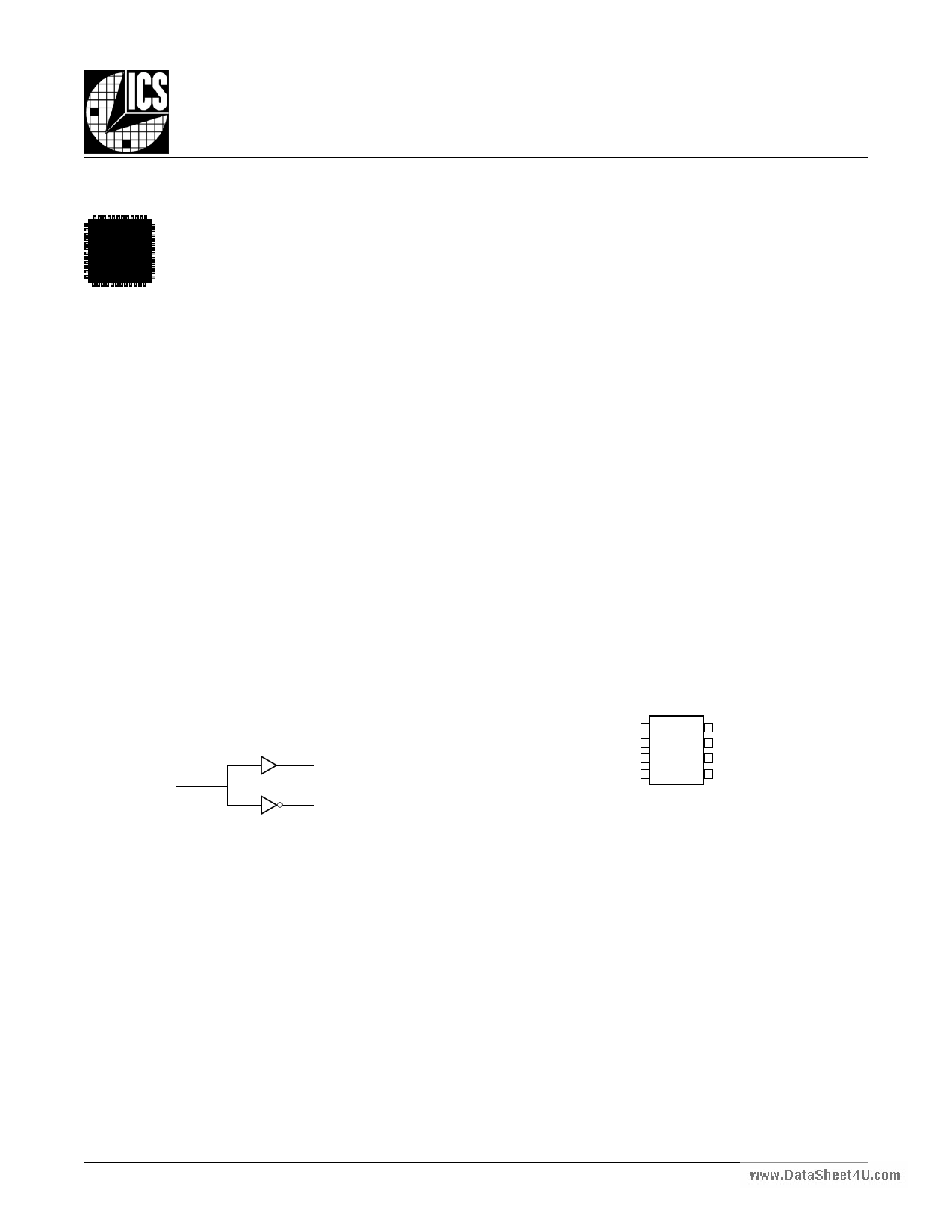
BLOCK DIAGRAM
CLK
Q
nQ
PIN ASSIGNMENT
VDDO
VDD
CLK
GND
1
2
3
4
8Q
7 GND
6 VDDO
5 nQ
ICS8302-01
8-Lead SOIC
3.8mm x 4.8mm, x 1.47mm package body
M Package
Top View
8302AM-01
www.icst.com/products/hiperclocks.html
1
REV. A DECEMBER 10, 2002
1 page 
Integrated
Circuit
Systems, Inc.
ICS8302-01
LOW SKEW, 1-TO-2 LVCMOS / LVTTL
FANOUT BUFFER W/ COMPLEMENTARY OUTPUT
PARAMETER MEASUREMENT INFORMATION
VDD, VDDO = 1.65V±5%
www.DataSheet4U.com
LVCMOS
2.05V±5% 1.25V±5%
SCOPE
Qx
VDD
VDDO
LVCMOS
SCOPE
Qx
GND = -1.65V±5%
3.3V OUTPUT LOAD AC TEST CIRCUIT
CLK
V
DD
2
V
DDO
Q2
nQ V
DDO
2
t
PD
PROPAGATION DELAY
PART 1
Q
PART 2
Q
nQ
V
DD
2
V
DDO
2
V
DDO
2
tsk(pp)
PART-TO-PART SKEW
GND = -1.25V±5%
3.3V/2.5V OUTPUT LOAD AC TEST CIRCUIT
V
DDO
Q2
nQ V
DDO
2
t sk(o)
OUTPUT SKEW
20%
Clock Outputs
80%
t
R
80%
t
F
20%
OUTPUT RISE/FALL TIME
nQ
VDDO
Q2
t PW
odc = t PW
t PERIOD
odc & t
PERIOD
8302AM-01
VDDO
2
t PERIOD
www.icst.com/products/hiperclocks.html
5
REV. A DECEMBER 10, 2002
5 Page | ||
| Páginas | Total 8 Páginas | |
| PDF Descargar | [ Datasheet ICS8302-01.PDF ] | |
Hoja de datos destacado
| Número de pieza | Descripción | Fabricantes |
| ICS8302-01 | 1-TO-2 LVCMOS / LVTTL FANOUT BUFFER W/ COMPLEMENTARY OUTPUT | Integrated Circuit Systems |
| Número de pieza | Descripción | Fabricantes |
| SLA6805M | High Voltage 3 phase Motor Driver IC. |
Sanken |
| SDC1742 | 12- and 14-Bit Hybrid Synchro / Resolver-to-Digital Converters. |
Analog Devices |
|
DataSheet.es es una pagina web que funciona como un repositorio de manuales o hoja de datos de muchos de los productos más populares, |
| DataSheet.es | 2020 | Privacy Policy | Contacto | Buscar |