|
|
|
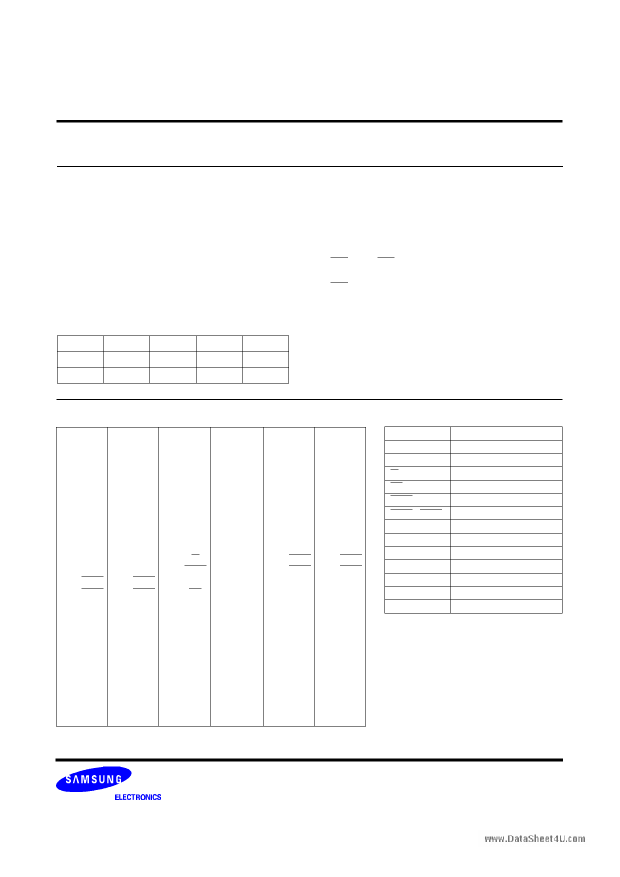
PDF KMM466F404BS2-L Data sheet ( Hoja de datos )
| Número de pieza | KMM466F404BS2-L | |
| Descripción | 4M X 64 DRAM SODIMM | |
| Fabricantes | Samsung Semiconductor | |
| Logotipo | ||
Hay una vista previa y un enlace de descarga de KMM466F404BS2-L (archivo pdf) en la parte inferior de esta página. Total 20 Páginas | ||
|
No Preview Available !
DRAM MODULE
KMM466F404BS2-L
KMM466F404BS2-L EDO Mode
4M x 64 DRAM SODIMM Using 4Mx16, 4K Refresh 3.3V, Low power/Self-Refresh
GENERAL DESCRIPTION
The Samsung KMM466F404BS2-L is a 4Mx64bits Dynamic
RAM high density memory module. The Samsung
KMM466F404BS2-L consists of four CMOS 4Mx16bits
www.DataSheeDt4RUA.cMoms in TSOP 400mil packages and a 2K EEPROM in 8-
pin TSSOP package mounted on a 144-pin glass-epoxy sub-
strate. A 0.1uF decoupling capacitor is mounted on the
printed circuit board for each DRAM. The KMM466F404BS2-L
is a Small Out-line Dual in-line Memory Module and is
intended for mounting into 144 pin edge connector sockets.
PERFORMANCE RANGE
Speed
tRAC
tCAC
-5
50ns
13ns
-6
60ns
15ns
tRC
84ns
104ns
tHPC
20ns
25ns
FEATURES
• Part Identification
- KMM466F404BS2-L(4096 cycles/128ms, TSOP, L-ver)
• Extended Data Out Mode Operation
• New JEDEC standard proposal with EEPROM
• Serial Presense Detect with EEPROM
• CAS-before-RAS Refresh capability
• Self -refresh capability
• RAS-only and Hidden refresh capability
• LVTTL compatible inputs and outputs
• Single +3.3V±0.3V power supply
• PCB : Height(1000mil), double sided component
PIN CONFIGURATIONS
Pin Front Pin Back Pin Front Pin Back Pin Front Pin Back
1 VSS 2 VSS 49 DQ13 50 DQ45 97 DQ22 98 DQ54
3 DQ0 4 DQ32 51 DQ14 52 DQ46 99 DQ23 100 DQ55
5 DQ1 6 DQ33 53 DQ15 54 DQ47 101 VCC 102 VCC
7 DQ2 8 DQ34 55 VSS 56 VSS 103 A6 104 A7
9 DQ3 10 DQ35 57 RSVD 58 RSVD 105 A8 106 A11
11 VCC 12 VCC 59 RSVD 60 RSVD 107 VSS 108 VSS
13 DQ4 14 DQ36 61 RFU 62 RFU 109 A9 110 NC
15 DQ5 16 DQ37 63 VCC 64 VCC 111 A10 112 NC
17 DQ6 18 DQ38 65 RFU 66 RFU 113 VCC 114 VCC
19 DQ7 20 DQ39 67 W 68 RFU 115 CAS2 116 CAS6
21 VSS 22 VSS 69 RAS0 70 RFU 117 CAS3 118 CAS7
23 CAS0 24 CAS4 71 NC 72 RFU 119 VSS 120 Vss
25 CAS1 26 CAS5 73 OE 74 RFU 121 DQ24 122 DQ56
27 VCC 28 VCC 75 VSS 76 VSS 123 DQ25 124 DQ57
29 A0 30 A3 77 RSVD 78 RSVD 125 DQ26 126 DQ58
31 A1 32 A4 79 RSVD 80 RSVD 127 DQ27 128 DQ59
33 A2 34 A5 81 VCC 82 VCC 129 VCC 130 VCC
35 VSS 36 VSS 83 DQ16 84 DQ48 131 DQ28 132 DQ60
37 DQ8 38 DQ40 85 DQ17 86 DQ49 133 DQ29 134 DQ61
39 DQ9 40 DQ41 87 DQ18 88 DQ50 135 DQ30 136 DQ62
41 DQ10 42 DQ42 89 DQ19 90 DQ51 137 DQ31 138 DQ63
43 DQ11 44 DQ43 91 VSS 92 VSS 139 VSS 140 Vss
45 VCC 46 VCC 93 DQ20 94 DQ52 141 SDA 142 SCL
47 DQ12 48 DQ44 95 DQ21 96 DQ53 143 VCC 144 VCC
PIN NAMES
Pin Name
Function
A0 to A11
Address Inputs
DQ0 - DQ63 Data In/Out
W Read/Write Enable
OE Output Enable
RAS0
Row Address Strobe
CAS0 - CAS7 Column Address Strobe
VCC Power(+3.3V)
VSS Ground
NC No Connection
SDA
Serial Address / Data I/O
SCL Serial Clock
RSVD
Reserved Use
RFU
Reserved for Future Use
1 page 
DRAM MODULE
KMM466F404BS2-L
AC CHARACTERISTICS (0°C≤TA≤70°C, VCC=3.3V±0.3V. See notes 1,2.)
Test condition : Vih/Vil=2.2/0.7V, Voh/Vol=2.0/0.8V, output loading CL=100pF
Parameter
Symbol
-5
Min Max
Column address to W delay time
CAS precharge to W delay time
CAS setup time (CAS-before-RAS refresh)
CAS hold time (CAS-before-RAS refresh)
www.DataSheet4RUA.cSomto CAS precharge time
Access time from CAS precharge
Hyper page mode cycle time
Hyper page mode read-modify write cycle time
CAS precharge time (Hyper page cycle)
RAS pulse width (Hyper page cycle)
RAS hold time from CAS precharge
W to RAS precharge time (C-B-R refresh)
W to RAS hold time (C-B-R refresh)
OE access time
OE to data delay
Output buffer turn off delay time from OE
OE command hold time
Output data hold time
Output buffer turn off delay from RAS
Output buffer turn off delay from W
W to data delay
OE to CAS hold time
CAS hold time to OE
OE precharge time
W pulse width(Hyper page cycle)
RAS pulse width (C-B-R self refresh)
RAS precharge time (C-B-R self refresh)
CAS hold time (C-B-R self refresh)
tAWD
tCPWD
tCSR
tCHR
tRPC
tCPA
tHPC
tHPRWC
tCP
tRASP
tRHCP
tWRP
tWRH
tOEA
tOED
tOEZ
tOEH
tDOH
tREZ
tWEZ
tWED
tOCH
tCHO
tOEP
tWPE
tRASS
tRPS
tCHS
45
47
5
10
5
28
20
67
7
50 200K
30
10
10
13
10
3 13
5
5
3 13
3 13
15
5
5
5
5
100
90
-50
-6
Min Max
53
58
5
10
5
35
25
73
10
60 200K
35
10
10
15
13
3 13
5
5
3 15
3 15
15
5
5
5
5
100
110
-50
Unit
Note
ns 6
ns 6
ns 16
ns 17
ns
ns 3
ns 10
ns 10
ns 13
ns
ns
ns
ns
ns 3
ns
ns
ns
ns
ns 11
ns
ns
ns
ns
ns
ns
us 19,20,21
ns 19,20,21
ns 19,20,21
5 Page 
DRAM MODULE
HYPER PAGE READ CYCLE
KMM466F404BS2-L
www.DataSheet4U.com
VIH -
RAS
VIL -
VIH -
CAS
VIL -
VIH -
A
VIL -
tRASP
tCRP
tCSH
tRCD
tHPC
tCP
tCAS
¡ó
tHPC
tCAS
tCP
tHPC
tCP
tCAS
tRHCP
tCAS
tRAD
tASR tRAH tASC tCAH tASC tCAH tASC tCAH tASC tCAH
ROW
ADDR
COLUMN
ADDRESS
COLUMN
ADDRESS
COLUMN
ADDR
COLUMN
ADDRESS
tRP
tREZ
VIH -
W
VIL -
VIH -
OE
VIL -
VOH -
DQ
VOL -
tRCS
tCAC
tAA
tCPA
tAA tCAC
tOEA
tRAC
tCAC
tDOH
VALID
DATA-OUT
tOLZ
tCLZ
VALID
DATA-OUT
tRCH
tRRH
tCAC
tAA
tCPA
tOCH
tOEA
tCPA
tCAC
tAA
tCHO
tOEP
tOEP
tOEZ
tOEZ
tOEA
VALID
DATA-OUT
tOEZ
VALID
DATA-OUT
Don′t care
Undefined
11 Page | ||
| Páginas | Total 20 Páginas | |
| PDF Descargar | [ Datasheet KMM466F404BS2-L.PDF ] | |
Hoja de datos destacado
| Número de pieza | Descripción | Fabricantes |
| KMM466F404BS2-L | 4M X 64 DRAM SODIMM | Samsung Semiconductor |
| Número de pieza | Descripción | Fabricantes |
| SLA6805M | High Voltage 3 phase Motor Driver IC. |
Sanken |
| SDC1742 | 12- and 14-Bit Hybrid Synchro / Resolver-to-Digital Converters. |
Analog Devices |
|
DataSheet.es es una pagina web que funciona como un repositorio de manuales o hoja de datos de muchos de los productos más populares, |
| DataSheet.es | 2020 | Privacy Policy | Contacto | Buscar |