|
|
|
PDF LH28F800SU Data sheet ( Hoja de datos )
| Número de pieza | LH28F800SU | |
| Descripción | 8M (512K bb 16/ 1M bb 8) Flash Memory | |
| Fabricantes | Sharp Electrionic Components | |
| Logotipo | ||
Hay una vista previa y un enlace de descarga de LH28F800SU (archivo pdf) en la parte inferior de esta página. Total 30 Páginas | ||
|
No Preview Available !
LH28F800SU
FEATURES
• User-Configurable x8 or x16 Operation
• User-Selectable 3.3 V or 5 V VCC
• 5 V Write/Erase Operations (5 V VPP)
– No Requirement for DC/DC
Converter to Write/Erase
• 70 ns Maximum Access Time
• Minimum 2.7 V Read capability
– 160 ns Maximum Access Time
(VCC = 2.7 V)
• 16 Independently Lockable Blocks
• 0.32 MB/sec Write Transfer Rate
• 100,000 Erase Cycles per Block
• Revolutionary Architecture
– Pipelined Command Execution
– Write During Erase
– Command Superset of
Sharp LH28F008SA
• 5 µA (TYP.) ICC in CMOS Standby
• 1 µA (TYP.) Deep Power-Down
• State-of-the-Art 0.55 µm ETOX™
Flash Technology
• 56-Pin, 1.2 mm × 14 mm × 20 mm
TSOP (Type I) Package
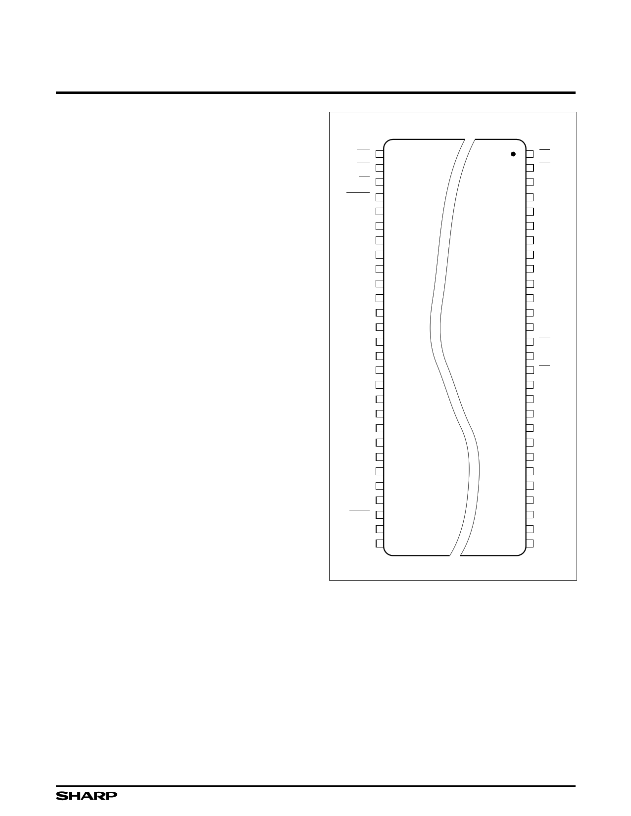
8M (512K × 16, 1M × 8) Flash Memory
56-PIN TSOP
TOP VIEW
WP
WE
OE
RY/BY
DQ15
DQ7
DQ14
DQ6
GND
DQ13
DQ5
DQ12
DQ4
VCC
GND
DQ11
DQ3
DQ10
DQ2
VCC
DQ9
DQ1
DQ8
DQ0
A0
BYTE
NC
NC
56
55
54
53
52
51
50
49
48
47
46
45
44
43
42
41
40
39
38
37
36
35
34
33
32
31
30
29
1 3/5
2 CE1
3 NC
4 NC
5 A19
6 A18
7 A17
8 A16
9 VCC
10 A15
11 A14
12 A13
13 A12
14 CE0
15 VPP
16 RP
17 A11
18 A10
19 A9
20 A8
21 GND
22 A7
23 A6
24 A5
25 A4
26 A3
27 A2
28 A1
28F800SUR-1
Figure 1. TSOP Reverse Bend Configuration
1
1 page 
8M (512K × 16, 1M × 8) Flash Memory
LH28F800SU
PIN DESCRIPTION (Continued)
SYMBOL
TYPE
WP INPUT
BYTE INPUT
3/5» INPUT
VPP
VCC
GND
NC
SUPPLY
SUPPLY
SUPPLY
NAME AND FUNCTION
WRITE PROTECT: Erase blocks can be locked by writing a non-volatile lock-bit for
each block. When WP is low, those locked blocks as reflected by the Block-Lock Status
bits (BSR.6), are protected from inadvertent Data Writes or Erases. When WP is high,
all blocks can be Written or Erased regardless of the state of the lock-bits. The WP
input buffer is disabled when RP» transitions low (deep power-down mode).
BYTE ENABLE: BYTE low places device x8 mode. All data is then input or output
on DQ0 - DQ7, and DQ8 - DQ15 float. Address A0 selects between the high and low
byte. BYTE high places the device in x16 mode, and turns off the A0 input buffer.
Address A1, then becomes the lowest order address.
3.3/5.0 VOLT SELECT: 3/5 » high configures internal circuits for 3.3 V operation.
3/5 » low configures internal circuits for 5.0 V operation.
NOTES: Reading the array with 3/5» high in a 5.0 V system could damage the
device. There is a significant delay from 3/5» switching to valid data.
ERASE/WRITE POWER SUPPLY (5.0 V ±0.5 V): For erasing memory array blocks or
writing words/bytes/pages into the flash array.
DEVICE POWER SUPPLY (3.3 V ±0.3 V, 5.0 V ±0.5 V) (2.7 ~ 3.6 at Read Operation):
Do not leave any power pins floating.
GROUND FOR ALL INTERNAL CIRCUITRY: Do not leave any ground pins floating.
NO CONNECT: No internal connection to die, lead may be driven or left floating.
5
5 Page 
8M (512K × 16, 1M × 8) Flash Memory
LH28F800SU
LH28F800SU Performance Enhancement Command Bus Definitions
COMMAND
FIRST BUS CYCLE SECOND BUS CYCLE
THIRD BUS CYCLE
MODE
OPER. ADDR. DATA OPER. ADDR. DATA OPER. ADDR. DATA
NOTE
Read Extended
Status Register
Write X
71H Read
RA
GSRD
BSRD
1
Page Buffer Swap
Write X 72H
7
Read Page Buffer
Write X 75H Read PA PD
Single Load to
Page Buffer
Write X 74H Write PA PD
x8 Write X E0H Write X BCL Write X
Sequential Load to
Page Buffer
x16 Write X E0H Write X WCL Write X
BCH
WCH
4, 6, 10
4, 5,
6, 10
Page Buffer Write
x8 Write
X
0CH Write
A0
BC
(L, H)
Write
WA
BC (H, L)
3, 4,
9, 10
to Flash
x16 Write X 0CH Write X WCL Write WA WCH 4, 5, 10
Two-Byte Write
x8 Write
X
FBH Write
A0
WD
(L, H)
Write
WA WD (H, L)
3
Block
Erase/Confirm
Write X 20H Write BA D0H
Lock Block/Confirm
Write X 77H Write BA D0H
Upload Status
Bits/Confirm
Write X 97H Write X D0H
2
Upload Device
Information
Write X 99H Write X D0H
Erase All Unlocked
Blocks/Confirm
Write X A7H Write X D0H
RY»/BY » Enable to
Level-Mode
Write X 96H Write X 01H
8
RY»/BY » Pulse-On-
Write
Write X 96H Write X 02H
8
RY»/BY » Pulse-On-
Erase
Write X 96H Write X 03H
8
RY»/BY » Disable
Write X 96H Write X 04H
8
Sleep
Write X F0H
Abort
Write X 80H
ADDRESS
BA = Block Address
PA = Page Buffer Address
RA = Extended Register Address
WA = Write Address
X = Don’t Care
DATA
AD = Array Data
PD = Page Buffer Data
BSRD = BSR Data
GSRD = GSR Data
WC (L, H) = Word Count (Low, High)
BC (L, H) = Byte Count (Low, High)
WD (L, H) = Write Data (Low, High)
11
11 Page | ||
| Páginas | Total 30 Páginas | |
| PDF Descargar | [ Datasheet LH28F800SU.PDF ] | |
Hoja de datos destacado
| Número de pieza | Descripción | Fabricantes |
| LH28F800SG | 8 M-bit (512 kB x 16) SmartVoltage Flash Memory | Sharp Electrionic Components |
| LH28F800SG | 8 M-bit (512 kB x 16) SmartVoltage Flash Memories | Sharp Electrionic Components |
| LH28F800SG-L | 8 M-bit (512 kB x 16) SmartVoltage Flash Memories | Sharp Electrionic Components |
| LH28F800SG-L | 8 M-bit (512 kB x 16) SmartVoltage Flash Memory | Sharp Electrionic Components |
| Número de pieza | Descripción | Fabricantes |
| SLA6805M | High Voltage 3 phase Motor Driver IC. |
Sanken |
| SDC1742 | 12- and 14-Bit Hybrid Synchro / Resolver-to-Digital Converters. |
Analog Devices |
|
DataSheet.es es una pagina web que funciona como un repositorio de manuales o hoja de datos de muchos de los productos más populares, |
| DataSheet.es | 2020 | Privacy Policy | Contacto | Buscar |