|
|
|
PDF LH28F400SU-LC Data sheet ( Hoja de datos )
| Número de pieza | LH28F400SU-LC | |
| Descripción | 4M (512K bb 8/ 256K bb 16) Flash Memory | |
| Fabricantes | Sharp Electrionic Components | |
| Logotipo | ||
Hay una vista previa y un enlace de descarga de LH28F400SU-LC (archivo pdf) en la parte inferior de esta página. Total 30 Páginas | ||
|
No Preview Available !
LH28F400SU-LC 4M (512K × 8, 256K × 16) Flash Memory
FEATURES
• User-Configurable x8 or x16 Operation
• 5 V Write/Erase Operation
(5 V VPP, 3.3 V VCC)
– No Requirement for DC/DC Converter
to Write/Erase
• 150 ns Maximum Access Time
(VCC = 3.3 V ± 0.3 V)
• Minimum 2.7 V Read Capability
– 190 ns Maximum Access Time
(VCC = 2.7 V)
• 32 Independently Lockable Blocks (16K)
• 100,000 Erase Cycles per Block
• Automated Byte Write/Block Erase
– Command User Interface
– Status Register
– RY /» BY » Status Output
• System Performance Enhancement
– Erase Suspend for Read
– Two-Byte Write
– Full Chip Erase
• Data Protection - Hardware Erase/Write
Lockout during Power Transitions
– Software Erase/Write Lockout
• Independently Lockable for Write/Erase
on Each Block (Lock Block and Protect
Set/Reset)
• 4 µA (Typ.) ICC in CMOS Standby
• 0.2 µA (Typ.) Deep Power-Down
• Extended Temperature Operation
– -40°C to +85°C
• State-of-the-Art 0.55 µm ETOX™ Flash
Technology
• 56-Pin, 1.2 mm × 14 mm × 20 mm TSOP
(Type I) Package
• 48-Pin 1.2 mm × 12 mm × 18 mm TSOP
(Type I) Package
• 44-Pin 600-mil SOP Package
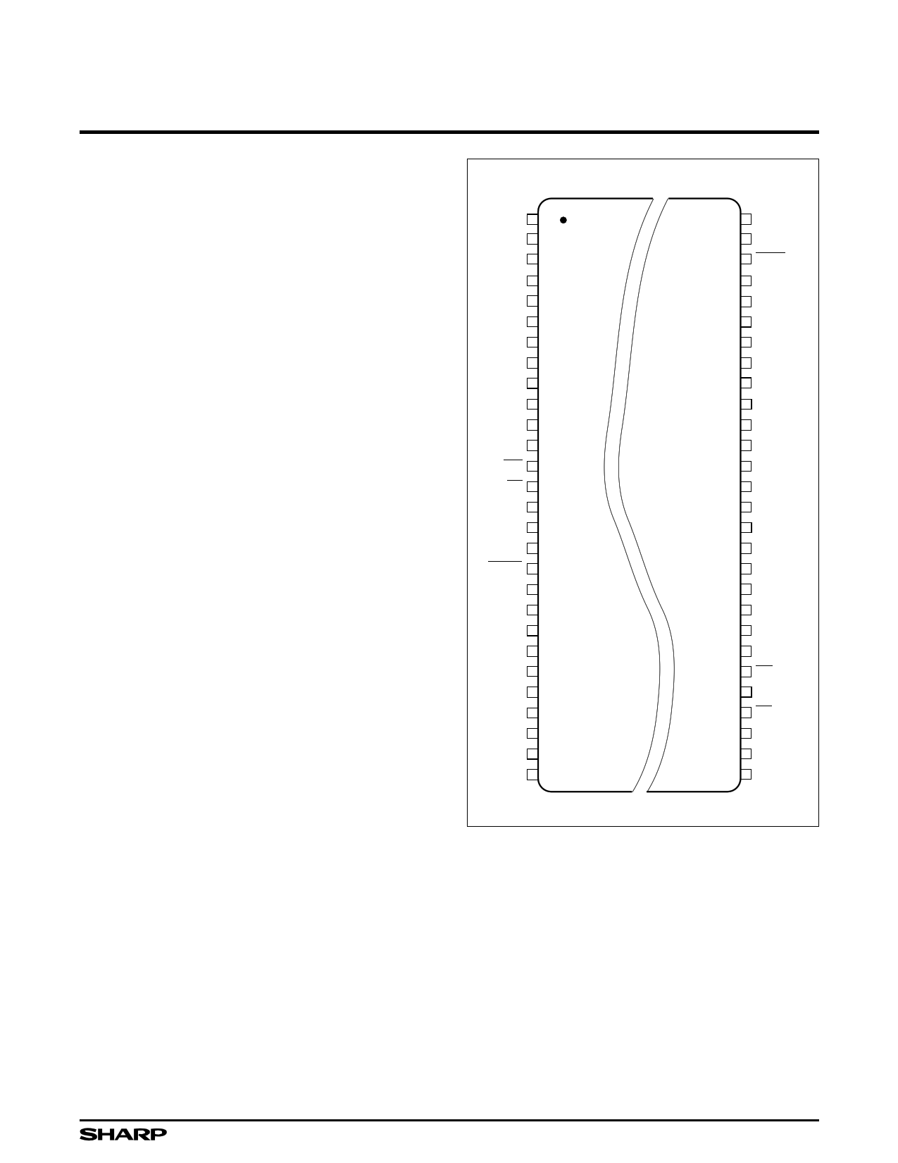
56-PIN TSOP
TOP VIEW
NC
NC
A15
A14
A13
A12
A11
A10
A9
A8
NC
NC
WE
RP
NC
NC
VPP
RY/BY
NC
A17
A7
A6
A5
A4
A3
A2
A1
NC
1
2
3
4
5
6
7
8
9
10
11
12
13
14
15
16
17
18
19
20
21
22
23
24
25
26
27
28
56 NC
55 A16
54 BYTE
53 GND
52 DQ15/A-1
51 DQ7
50 DQ14
49 DQ6
48 DQ13
47 DQ5
46 DQ12
45 DQ4
44 VCC
43 VCC
42 DQ11
41 DQ3
40 DQ10
39 DQ2
38 DQ9
37 DQ1
36 DQ8
35 DQ0
34 QE
33 GND
32 CE
31 A0
30 NC
29 NC
28F400SUH-LC15-1
Figure 1. 56-Pin TSOP Configuration
1
1 page 
4M (512K × 8, 256K × 16) Flash Memory
LH28F400SU-LC
INTRODUCTION
Sharp’s LH28F400SU-LC 4M Flash Memory is a
revolutionary architecture which enables the design of
truly mobile, high performance, personal computing and
communication products. With innovative capabilities,
3.3 V low power operation and very high read/write per-
formance, the LH28F400SU-LC is also the ideal choice
for designing embedded mass storage flash memory
systems.
The LH28F400SU-LC’s independently lockable 32
symmetrical blocked architecture (16K each) extended
cycling, low power operation, very fast write and read
performance and selective block locking provide a highly
flexible memory component suitable for cellular phone,
facsimile, game, PC, printer and handy terminal. The
LH28F400SU-LC’s 5.0 V/3.3 V power supply operation
enables the design of memory cards which can be read
in 3.3 V system and written in 5.0 V/3.3 V systems. Its
x8/x16 architecture allows the optimization of memory
to processor interface. The flexible block locking option
enables bundling of executable application software in
a Resident Flash Array or memory card. Manufactured
on Sharp’s 0.55 µm ETOX™ process technology, the
LH28F400SU-LC is the most cost-effective, high-
density 3.3 V flash memory.
DESCRIPTION
The LH28F400SU-LC is a high performance
4M (4,194,304 bit) block erasable non-volatile random
access memory organized as either 256K × 16 or
512K × 8. The LH28F400SU-LC includes thirty-two
16K (16,384) blocks. A chip memory map is shown in
Figure 5.
The implementation of a new architecture, with many
enhanced features, will improve the device operating
characteristics and results in greater product reliability
and ease of use.
Among the significant enhancements of the
LH28F400SU-LC:
• 3 V Read, 5 V Write/Erase Operation
(5 V VPP, 3 V VCC)
• Low Power Capability (2.7 V VCC Read)
• Improved Write Performance
• Dedicated Block Write/Erase Protection
• Command-Controlled Memory Protection
Set/Reset Capability
A Command User Interface (CUI) serves as the sys-
tem interface between the microprocessor or
microcontroller and the internal memory operation.
Internal Algorithm Automation allows ByteWrites and
Block Erase operations to be executed using a Two-
Write command sequence to the CUI in the same way
as the LH28F008SA 8M Flash memory.
A Superset of commands have been added to the
basic LH28F008SA command-set to achieve higher
write performance and provide additional capabilities.
These new commands and features include:
• Software Locking of Memory Blocks
• Memory Protection Set/Reset Capability
• Two-Byte Serial Writes in 8-bit Systems
• Erase All Unlocked Blocks
Writing of memory data is performed typically within
20 µs per byte. Writing of memory data is performed
typically within 30 µs per word. A Block Erase operation
erases one of the 32 blocks in typically 0.8 seconds,
independent of the other blocks.
LH28F400SU-LC allows to erase all unlocked blocks.
It is desirable in case of which you have to implement
Erase operation maximum 32 times.
LH28F400SU-LC enable Two-Byte serialWrite which
is operated by three times command imput. Writing of
memory data is performed typically within 30 µs per
two-byte. This feature can improve 8-bit system write
performance by up to typically 15 µs per byte.
All operations are started by a sequence of Write
commands to the device. Status Register (described in
detail later) and a RY »/BY » output pin provide informa-
tion on the progress of the requested operation.
Same as the LH28F008SA, LH28F400SU-LC
requires an operation to complete before the next
operation can be requested, also it allows to suspend
block erase to read data from any other block, and
allow to resume erase operation.
The LH28F400SU-LC provides user-selectable block
locking to protect code or data such as Device Drivers,
PCMCIA card information, ROM-Executable OS or
Application Code. Each block has an associated non-
volatile lock-bit which determines the lock status of the
block. In addition, the LH28F400SU-LC has a software
controlled master Write Protect circuit which prevents
any modifications to memory blocks whose lock-bits
are set.
5
5 Page 
4M (512K × 8, 256K × 16) Flash Memory
LH28F400SU-LC
START
WRITE 20H
WRITE D0H AND
BLOCK ADDRESS
READ COMPATIBLE
STATUS REGISTER
SUSPEND
NO ERASE LOOP
0
CSR.7 =
SUSPEND YES
ERASE
1
CSR FULL STATUS
CHECK IF DESIRED
BUS
OPERATION
COMMAND
COMMENTS
Write
Write
Read
Block Erase D = 20H
A=X
Confirm
D = D0H
A = BA
Q = CSRD
Toggle CE or OE
to update CSRD.
A=X
Standby
Check CSR.7
1 = WSM Ready
0 = WSM Busy
Repeat for subsequent Block Erasures.
CSR Full Status Check can be done after each Block Erase,
or after a sequence of Block Erasures.
Write FFH after the last operation to reset
device to read array mode.
See Command Bus Cycle notes for description of codes.
OPERATION
COMPLETE
CSR FULL STATUS CHECK PROCEDURE
READ CSRD
(see above)
0
CSR.4, 5 =
1
1
CSR.3 =
0
CLEAR CSRD
RETRY/ERROR
RECOVERY
ERASE
SUCCESSFUL
VPP LOW
DETECT
BUS
OPERATION
COMMAND
COMMENTS
Standby
Check CSR.4, 5
1 = Erase Error
0 = Erase Successful
Both 1 = Command
Sequence Error
Standby
Check CSR.3
1 = VPP Low Detect
0 = VPP OK
CSR.3, 4, 5 should be cleared, if set, before further attempts
are initiated.
Figure 7. Block Erase with Compatible Status Register
28F400SUH-LC15-5
11
11 Page | ||
| Páginas | Total 30 Páginas | |
| PDF Descargar | [ Datasheet LH28F400SU-LC.PDF ] | |
Hoja de datos destacado
| Número de pieza | Descripción | Fabricantes |
| LH28F400SU-LC | 4M (512K bb 8/ 256K bb 16) Flash Memory | Sharp Electrionic Components |
| Número de pieza | Descripción | Fabricantes |
| SLA6805M | High Voltage 3 phase Motor Driver IC. |
Sanken |
| SDC1742 | 12- and 14-Bit Hybrid Synchro / Resolver-to-Digital Converters. |
Analog Devices |
|
DataSheet.es es una pagina web que funciona como un repositorio de manuales o hoja de datos de muchos de los productos más populares, |
| DataSheet.es | 2020 | Privacy Policy | Contacto | Buscar |