|
|
|
PDF LH28F016SA Data sheet ( Hoja de datos )
| Número de pieza | LH28F016SA | |
| Descripción | 16M (1M bb 16/ 2M bb 8) Flash Memory | |
| Fabricantes | Sharp Electrionic Components | |
| Logotipo | ||
Hay una vista previa y un enlace de descarga de LH28F016SA (archivo pdf) en la parte inferior de esta página. Total 30 Páginas | ||
|
No Preview Available !
LH28F016SA
FEATURES
• User-Configurable x8 or x16 Operation
• User-Selectable 3.3 V or 5 V VCC
• 70 ns Maximum Access Time
• 0.43 MB/sec Write Transfer Rate
• 100,000 Erase Cycles per Block
• 32 Independently Lockable Blocks (64K)
• Revolutionary Architecture
– Pipelined Command Execution
– Write During Erase
– Command Superset of
Sharp LH28F008SA
• 50 µA (Typ.) ICC in CMOS Standby
• 1 µA (Typ.) Deep Power-Down
• State-of-the-Art 0.55 µm ETOX™ Flash
Technology
• 56-Pin, 1.2 mm × 14 mm × 20 mm
TSOP (Type I) Package
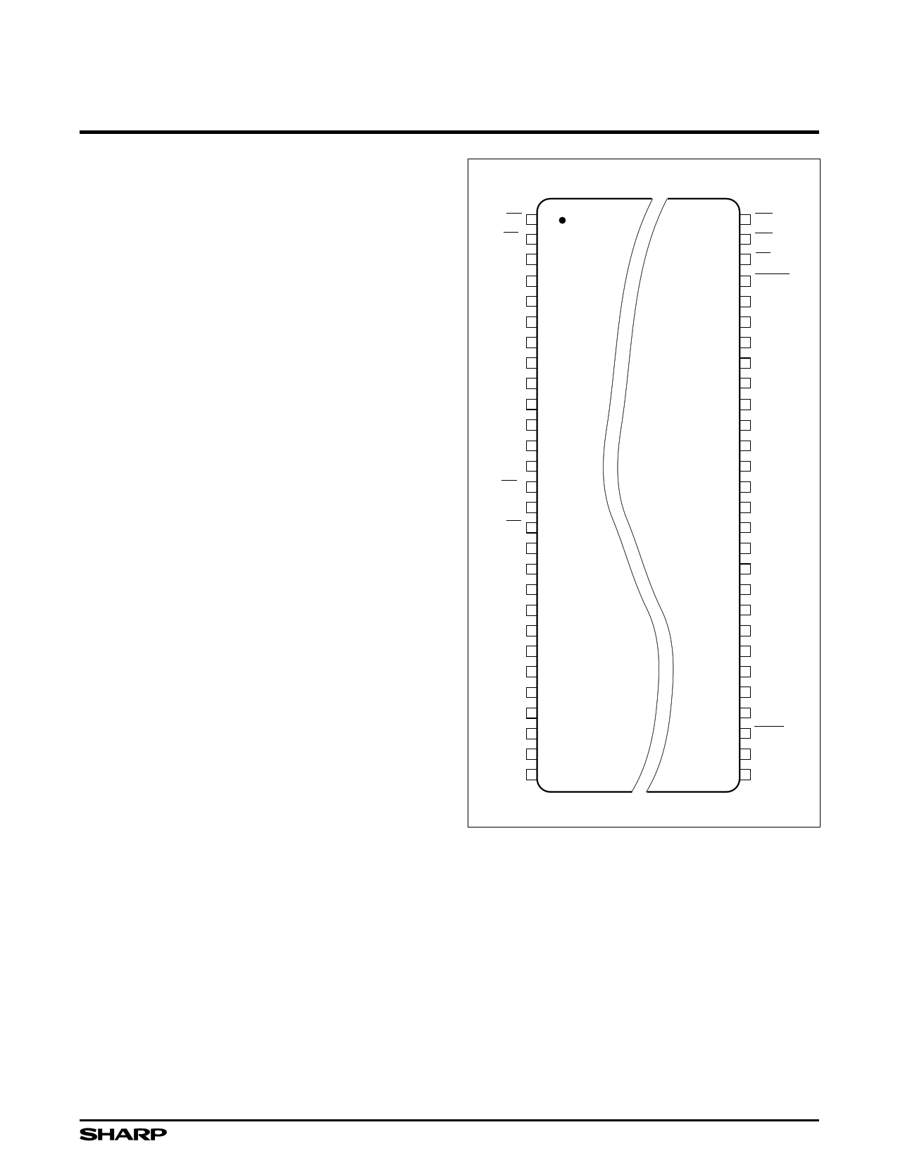
16M (1M × 16, 2M × 8) Flash Memory
56-PIN TSOP
TOP VIEW
3/5
CE1
NC
A20
A19
A18
A17
A16
VCC
A15
A14
A13
A12
CE0
VPP
RP
A11
A10
A9
A8
GND
A7
A6
A5
A4
A3
A2
A1
1
2
3
4
5
6
7
8
9
10
11
12
13
14
15
16
17
18
19
20
21
22
23
24
25
26
27
28
56 WP
55 WE
54 OE
53 RY/BY
52 DQ15
51 DQ7
50 DQ14
49 DQ6
48 GND
47 DQ13
46 DQ5
45 DQ12
44 DQ4
43 VCC
42 GND
41 DQ11
40 DQ3
39 DQ10
38 DQ2
37 VCC
36 DQ9
35 DQ1
34 DQ8
33 DQ0
32 A0
31 BYTE
30 NC
29 NC
28F016SAT-1
Figure 1. TSOP Configuration
1
1 page 
16M (1M × 16, 2M × 8) Flash Memory
LH28F016SA
A Command User Interface (CUI) serves as the sys-
tem interface between the microprocessor or
microcontroller and the internal memory operation.
Internal Algorithm Automation allows Byte/Word
Writes and Block Erase operations to be executed
using a Two-Write command sequence to the CUI in
the same way as the LH28F008SA 8M Flash memory.
A Superset of commands have been added to the
basic LH28F008SA command-set to achieve higher
write performance and provide additional capabilities.
These new commands and features include:
• Page Buffer Writes to Flash
• Command Queuing Capability
• Automatic Data Writes During Erase
• Software Locking of Memory Blocks
• Two-Byte Successive Writes in 8-bit Systems
• Erase All Unlocked Blocks
Writing of memory data is performed in either byte or
word increments typically within 6 µs, a 33% improve-
ment over the LH28F008SA. A Block Erase operation
erases one of the 32 blocks in typically 0.6 seconds,
independent of the other blocks, which is about 65%
improvement over the LH28F008SA.
The LH28F016SA incorporates two Page Buffers of
256 Bytes (128 Words) each to allow page data writes.
This feature can improve a system write performance
over previous flash memory devices.
All operations are started by a sequence of Write
commands to the device. Three Status Registers (de-
scribed in detail later) and a RY »/BY » output pin provide
information on the progress of the requested operation.
While the LH28F008SA requires an operation to com-
plete before the next operation can be requested, the
LH28F016SA allows queuing of the next operation while
the memory executes the current operation. This elimi-
nates system overhead when writing several bytes in a
row to the array or erasing several blocks at the same
time. The LH28F016SA can also perform write opera-
tions to one block of memory while performing erase of
another block.
The LH28F016SA provides user-selectable block
locking to protect code or data such as Device Drivers,
PCMCIA card information, ROM-Executable O/S or
Application Code. Each block has an associated non-
volatile lock-bit which determines the lock status of the
block. In addition, the LH28F016SA has a master Write
Protect pin (WP ») which prevents any modifications to
memory blocks whose lock-bits are set.
The LH28F016SA contains three types of Status
Registers to accomplish various functions:
• A Compatible Status Register (CSR) which is 100%
compatible with the LH28F008SA Flash memory’s
Status Register.This register, when used alone, pro-
vides a straightforward upgrade capability to the
LH28F016SA from a LH28F008SA-based design.
• A Global Status Register (GSR) which informs the
system of command Queue status, Page Buffer sta-
tus, and overall Write State Machine (WSM) status.
• 32 Block Status Registers (BSRs) which provide
block-specific status information such as the block
lock-bit status.
The GSR and BSR memory maps for Byte-Wide and
Word-Wide modes are shown in Figures 4 and 5.
The LH28F016SA incorporates an open drain
RY »/BY » outpin. This feature allows the user to OR-tie
many RY »/BY » pins together in a multiple memory con-
figuration such as a Resident Flash Array.
The LH28F016SA also incorporates a dual chip-
enable function with two input pins, CE 0» and CE 1» .These
pins have exactly the same functionality as the regular
chip-enable pin CE » on the LH28F008SA. For minimum
chip designs, CE »1 may be tied to ground and use CE »0
as the chip enable input. The LH28F016SA uses the
logical combination of these two signals to enable or
disable the entire chip. Both CE »0 and CE »1 must be ac-
tive low to enable the device and if either one becomes
inactive, the chip will be disabled. This feature, along
with the open drain RY »/BY » pin, allows the system de-
signer to reduce the number of control pins used in a
large array of 16M devices.
The BY T» E » pin allows either x8 or x16 read/writes to
the LH28F016SA. BY T» E » at logic low selects 8-bit mode
with address A0 selecting between low byte and high
byte. On the other hand, BY T» E » at logic high enables
16-bit operation with address A1 becoming the lowest
order address and address A0 is not used (don’t care).
A block diagram is shown in Figure 2.
The LH28F016SA is specified for a maximum access
time of each version, as follows:
OPERATING
TEMPERATURE
0 - 70°C
0 - 70°C
0 - 70°C
VCC SUPPLY
4.75 - 5.25 V
4.5 - 5.5 V
3.0 - 3.6 V
MAX. ACCESS
(TACC)
70 ns
80 ns
120 ns
5
5 Page 
16M (1M × 16, 2M × 8) Flash Memory
LH28F016SA
NOTES:
1. RA can be the GSR address or any BSR address. See Figure 4 and 5 for Extended Status Register Memory Maps.
2. Upon device power-up, all BSR lock-bits come up locked. The Uploaded Status Bits command must be written to reflect the actual
lock-bit status.
3. A0 is automatically complemented to load second byte of data. BY T» E » must be at VIL. A0 value determines which WD/BC is supplied
first: A0 = 0 looks at the WDL/BCL, A0 = 1 looks at the WDH/BCH.
4. BCH/WCH must be at 00H for this product because of the 256-Byte (128 Word) Page Buffer size and to avoid writing the Page Buffer
contents into more than one 256-Byte segment within an array block. They are simply shown for future Page Buffer expandability.
5. In x16 mode, only the lower byte DQ0 - DQ7 is used for WCL and WCH. The upper byte DQ8 - DQ15 is a don’t care.
6. PA and PD (Whose count is given in cycles 2 and 3) are supplied starting in the 4th cycle which is not shown.
7. This command allows the user to swap between available Page Buffers (0 or 1).
8. These commands reconfigure RY »/BY » output to one of two pulse-modes or enable and disable the RY »/BY » function.
9. Write address, WA, is the Destination address in the flash array which must match the Source address in the Page Buffer. Refer to the
LH28F016SU User’s Manual.
10. BCL = 00H corresponds to a Byte count of 1. Similarly, WCL = 00H corresponds to a Word count of 1.
11. Unless you issue erase suspend command, it is not necessary to input D0H on third bus cycle.
Compatible Status Register
WSMS
ESS
ES
DWS
VPPS
R
R
R
76543210
CSR.7 = WRITE STATE MACHINE STATUS (WSMS)
1 = Ready
0 = Busy
CSR.6 = ERASE-SUSPEND STATUS (ESS)
1 = Erase Suspended
0 = Erase in Progress/Completed
CSR.5 = ERASE STATUS (ES)
1 = Error in Block Erasure
0 = Successful Block Erase
CSR.4 = DATA-WRITE STATUS (DWS)
1 = Error in Data Write
0 = Data Write Successful
CSR.3 = VPP STATUS (VPPS)
1 = VPP Low Detect, Operation Abort
0 = VPP OK
NOTES:
1. RY »/BY » output or WSMS bit must be checked to determine
completion of an operation (Erase Suspend, Erase or Data
Write) before the appropriate Status bit (ESS, ES or DWS)
is checked for success.
2. If DWS and ES are set to ‘1’ during an erase attempt, an
improper command sequence was entered. Clear the CSR
and attempt the operation again.
3. The VPPS bit, unlike an A/D converter, does not provide
continuous indication of VPP level. The WSM interrogates
VPP’s level only after the Data-Write or Erase command
sequences have been entered, and informs the system if
VPP has not been switched on. VPPS is not guaranteed to
report accurate feedback between VPPL and VPPH.
4. CSR.2 - CSR.0 = Reserved for future enhancements.
These bits are reserved for future use and should be
masked out when polling the CSR.
11
11 Page | ||
| Páginas | Total 30 Páginas | |
| PDF Descargar | [ Datasheet LH28F016SA.PDF ] | |
Hoja de datos destacado
| Número de pieza | Descripción | Fabricantes |
| LH28F016SA | 16M (1M bb 16/ 2M bb 8) Flash Memory | Sharp Electrionic Components |
| LH28F016SANS | 16 Mbit(1 Mbit x 16/ 2 Mbit x 8) | Sharp Electrionic Components |
| LH28F016SANS-70 | 16 Mbit(1 Mbit x 16/ 2 Mbit x 8) | Sharp Electrionic Components |
| LH28F016SC-L | 16 M-bit (2 MB x 8) SmartVoltage Flash Memories | Sharp Electrionic Components |
| Número de pieza | Descripción | Fabricantes |
| SLA6805M | High Voltage 3 phase Motor Driver IC. |
Sanken |
| SDC1742 | 12- and 14-Bit Hybrid Synchro / Resolver-to-Digital Converters. |
Analog Devices |
|
DataSheet.es es una pagina web que funciona como un repositorio de manuales o hoja de datos de muchos de los productos más populares, |
| DataSheet.es | 2020 | Privacy Policy | Contacto | Buscar |