|
|
|
PDF DS14287 Data sheet ( Hoja de datos )
| Número de pieza | DS14287 | |
| Descripción | (DS14285 / DS14287) Real-Time Clock | |
| Fabricantes | Real-Time Clock | |
| Logotipo | ||
Hay una vista previa y un enlace de descarga de DS14287 (archivo pdf) en la parte inferior de esta página. Total 26 Páginas | ||
|
No Preview Available !
www.maxim-ic.com
FEATURES
Direct Replacement for IBM AT
Computer Clock/Calendar
Functionally Compatible with the
DS1285/DS1287
Available as Chip (DS14285, DS14285S, or
DS14285Q) or Stand-Alone Module with
Embedded Lithium Battery and Crystal
(DS14287)
Automatic Backup Supply and Write
www.DataShPereott4eUc.tcionmto Make External SRAM
Nonvolatile
Counts Seconds, Minutes, Hours, Days,
Day of the Week, Date, Month, and Year
with Leap Year Compensation Valid Up
to 2100
Binary or BCD Representation of Time,
Calendar, and Alarm
12- or 24-Hour Clock with AM and PM in
12-Hour Mode
Daylight Saving Time Option
Multiplex Bus for Pin Efficiency
Interfaced with Software as 128 RAM
Locations
14 Bytes of Clock and Control Registers
114 Bytes of General Purpose RAM
Programmable Square-Wave Output
Signal
Bus-Compatible Interrupt Signals (IRQ)
Three Interrupts are Separately Software-
Maskable and Testable
Time-of-Day Alarm Once/Second to
Once/Day
Periodic Rates from 122µs to 500ms
End of Clock Update Cycle
Optional Industrial Temperature Version
Available: DS14285 DIP, SO, and PLCC
DS14285/DS14287
Real-Time Clock with NV RAM
Control Control
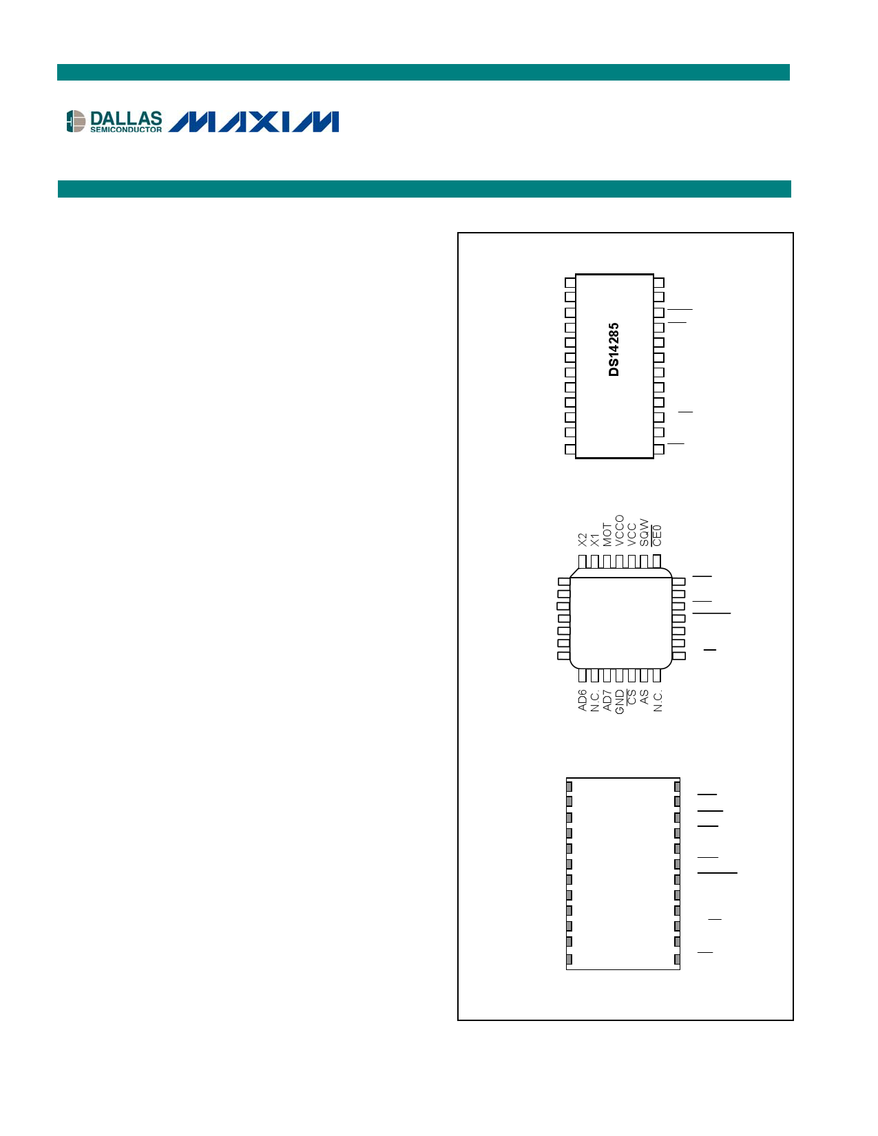
PIN CONFIGURATIONS
TOP VIEW
VCCO
X1
X2
AD0
AD1
AD2
AD3
AD4
AD5
AD6
AD7
GND
1 24
2 23
3 22
4 21
5 20
6 19
7 18
8 17
9 16
10 15
11 14
12 13
DIP/SO
VCC
SQW
CEO
CEI
VBAT
IRQ
RESET
DS
GND
R/W
AS
CS
AD0
AD1
AD2
AD3
AD4
AD5
N.C.
4 3 2 1 28 27 26
5 25
6 24
7 DS14285 23
8 22
9 21
10 20
11 19
12 13 14 15 16 17 18
CEI
VBAT
IRQ
RESET
DS
GND
R/W
PLCC
VCCO
N.C.
N.C.
AD0
AD1
AD2
AD3
AD4
AD5
AD6
AD7
GND
1 24
2
3
23
DS14287 22
4 21
5 20
6 19
7 18
8 17
9 16
10 15
11 14
12 13
VCC
SQW
CEO
CEI
N.C.
IRQ
RESET
DS
N.C.
R/W
AS
CS
Encapsulated Package
1 of 26
REV: 112105
1 page 
DS14285/DS14287
RESET (Reset Input) - The RESET pin has no effect on the clock, calendar, or RAM. On power-up the
RESET pin can be held low for a time in order to allow the power supply to stabilize. The amount of time
that RESET is held low is dependent on the application. However, if RESET is used on power-up, the
time RESET is low should exceed 200 ms to make sure that the internal timer that controls the
DS14285/DS14287 on power-up has timed out. When RESET is low and VCC is above 4.25 volts, the
following occurs:
A. Periodic Interrupt Enable (PEI) bit is cleared to 0.
B. Alarm Interrupt Enable (AIE) bit is cleared to 0.
C. Update Ended Interrupt Flag (UF) bit is cleared to 0.
D. Interrupt Request Status Flag (IRQF) bit is cleared to 0.
E. Periodic Interrupt Flag (PF) bit is cleared to 0.
F. The device is not accessible until RESET is returned high.
G. Alarm Interrupt Flag (AF) bit is cleared to 0.
www.DataSheet4U.comH. IRQ pin is in the high impedance state.
I. Square Wave Output Enable ( SQWE ) bit is cleared to 0.
J. Update Ended Interrupt Enable (UIE) is cleared to 0.
K. CEO is driven high.
In a typical application RESET can be connected to VCC. This connection will allow the DS14287 to go in
and out of power fail without affecting any of the control registers.
CEI (External RAM Chip Enable Input, active low) - CEI should be driven low to enable the external
RAM. CEI is internally pulled up with a 50kΩ resistor.
CEO (External RAM Chip Enable Output, active low) - When VCC is greater than 4.25 volts (typical),
CEO will reflect CEI provided the RESET is at a logic high. When VCC is less than 4.25 volts (typical),
CEO will be forced to an inactive level regardless of CEI .
VCCO (External RAM Power Supply Output) - VCCO provides the higher of VCC or VBAT through an
internal switch to power an external RAM.
DS14285 Only
X1, X2 - Connections for a standard 32.768 kHz quartz crystal. The internal oscillator circuitry is
designed for operation with a crystal having a specified load capacitance (CL) of 6 pF. The crystal is
connected directly to the X1 and X2 pins. There is no need for external capacitors or resistors. Note: X1
and X2 are very high impedance nodes. It is recommended that they and the crystal be guard–ringed with
ground and that high frequency signals be kept away from the crystal area. For more information on
crystal selection and crystal layout considerations, please consult Application Note 58, “Crystal
Considerations with Dallas Real Time Clocks.”
VBAT – Battery input for any standard 3-volt lithium cell or other energy source. See the Power-Up/Down
section for considerations in selecting the size of the external energy source
5 of 26
5 Page 
DS14285/DS14287
REGISTER B
MSB
BIT 7
BIT 6
SET PIE
BIT 5
AIE
BIT 4
UIE
BIT 3
SQWE
BIT 2
DM
BIT 1
24/12
LSB
BIT 0
DSE
SET - When the SET bit is a 0, the update transfer functions normally by advancing the counts once per
second. When the SET bit is written to a 1, any update transfer is inhibited and the program can initialize
the time and calendar bytes without an update occurring in the midst of initializing. Read cycles can be
executed in a similar manner. SET is a read/write bit that is not modified by RESET or internal functions
of the DS14285/DS14287.
PIE - The periodic interrupt enable PIE bit is a read/write bit which allows the Periodic Interrupt Flag
(PF) bit in Register C to drive the IRQ pin low. When the PIE bit is set to 1, periodic interrupts are
generated by driving the IRQ pin low at a rate specified by the RS3-RS0 bits of Register A. A 0 in the
PIE bit blocks the IRQ output from being driven by a periodic interrupt, but the Periodic Flag (PF) bit is
www.DatsatSillheseett4aUt.cthoemperiodic rate. PIE is not modified by any internal DS14285/DS14287 functions, but is
cleared to 0 on RESET .
AIE - The Alarm Interrupt Enable (AIE) bit is a read/write bit which, when set to a 1, permits the Alarm
Flag (AF) bit in register C to assert IRQ . An alarm interrupt occurs for each second that the 3 time bytes
equal the 3 alarm bytes including a “don’t care” alarm code of binary 11XXXXXX. When the AIE bit is
set to 0, the AF bit does not initiate the IRQ signal. The RESET pin clears AIE to 0. The internal
functions of the DS14285/DS14287 do not affect the AIE bit.
UIE - The Update Ended Interrupt Enable (UIE) bit is a read/write that enables the Update End Flag (UF)
bit in Register C to assert IRQ . The RESET pin going low or the SET bit going high clears to UIE bit.
SQWE - When the Square Wave Enable (SQWE) bit is set to a 1, a square wave signal at the frequency
set by the rate-selection bits RS3 through RS0 is driven out on a SQW pin. When the SQWE bit is set to
0, the SQW pin is held low; the state of SQWE is cleared by the RESET pin. SQWE is a read/write bit.
DM - The Data Mode (DM) bit indicates whether time and calendar information is in binary or BCD
format. The DM bit is set by the program to the appropriate format and can be read as required. This bit is
not modified by internal functions or RESET . A one in DM signifies binary data while a 0 in DM
specifies Binary Coded Decimal (BCD) data.
24/12 - The 24/12 control bit establishes the format of the hours byte. A 1 indicates the 24-hour mode and
a 0 indicates the 12-hour mode. This bit is read/write and is not affected by internal functions of RESET .
DSE - The Daylight Savings Enable (DSE) bit is a read/write bit which enables two special updates when
DSE is set to 1. On the first Sunday in April the time increments from 1:59:59 AM to 3:00:00 AM. On
the last Sunday in October when the time first reaches 1:59:59 AM it changes to 1:00:00 AM. These
special updates do not occur when the DSE bit is a 0. This bit is not affected by internal functions or
RESET .
11 of 26
11 Page | ||
| Páginas | Total 26 Páginas | |
| PDF Descargar | [ Datasheet DS14287.PDF ] | |
Hoja de datos destacado
| Número de pieza | Descripción | Fabricantes |
| DS14285 | (DS14285 / DS14287) Real-Time Clock | Real-Time Clock |
| DS14287 | (DS14285 / DS14287) Real-Time Clock | Real-Time Clock |
| Número de pieza | Descripción | Fabricantes |
| SLA6805M | High Voltage 3 phase Motor Driver IC. |
Sanken |
| SDC1742 | 12- and 14-Bit Hybrid Synchro / Resolver-to-Digital Converters. |
Analog Devices |
|
DataSheet.es es una pagina web que funciona como un repositorio de manuales o hoja de datos de muchos de los productos más populares, |
| DataSheet.es | 2020 | Privacy Policy | Contacto | Buscar |