|
|
|
PDF LM2655 Data sheet ( Hoja de datos )
| Número de pieza | LM2655 | |
| Descripción | 2.5A High Efficiency Synchronous Switching Regulator | |
| Fabricantes | National Semiconductor | |
| Logotipo | ||
Hay una vista previa y un enlace de descarga de LM2655 (archivo pdf) en la parte inferior de esta página. Total 16 Páginas | ||
|
No Preview Available !
February 2000
LM2655
2.5A High Efficiency Synchronous Switching Regulator
General Description
The LM2655 is a current-mode controlled PWM step-down
switching regulator. It has the unique ability to operate in
synchronous or asynchronous mode. This gives the de-
signer flexibility to choose between the high efficiency of
synchronous operation, or the low solution cost of asynchro-
nous operation. Along with flexibility, the LM2655 offers high
power density with the small footprint of a TSSOP-16 pack-
age.
High efficiency (>90%) is obtained through the use of an in-
ternal low ON-resistance (33mΩ) MOSFET, and an external
N-Channel MOSFET. This feature, together with its low qui-
escent current, makes the LM2655 an ideal fit in portable ap-
plications.
Integrated in the LM2655 are all the power, control, and drive
functions for asynchronous operation. In addition, a low-side
driver output allows easy synchronous operation. The IC
uses patented current sensing circuitry that eliminates the
external current sensing resistor required by other current-
mode DC-DC converters. A programmable soft-start feature
limits start up current surges and provides a means of se-
quencing multiple power supplies.
Features
n Ultra-high efficiency up to 96%
n 4V to 14V input voltage range
n Internal high-side MOSFET with low RDS(ON) = 0.033Ω
n 300 kHz fixed frequency internal oscillator
n Low-side drive for synchronous operation
n Guaranteed less than 12 µA shutdown current
n Patented current sensing for current mode control
n Programmable soft-start
n Input undervoltage lockout
n Output overvoltage shutdown protection
n Output undervoltage shutdown protection
n Thermal Shutdown
n 16-pin TSSOP package
Applications
n Hard disk drives
n Internet appliances
n TFT monitors
n Computer peripherals
n Battery powered devices
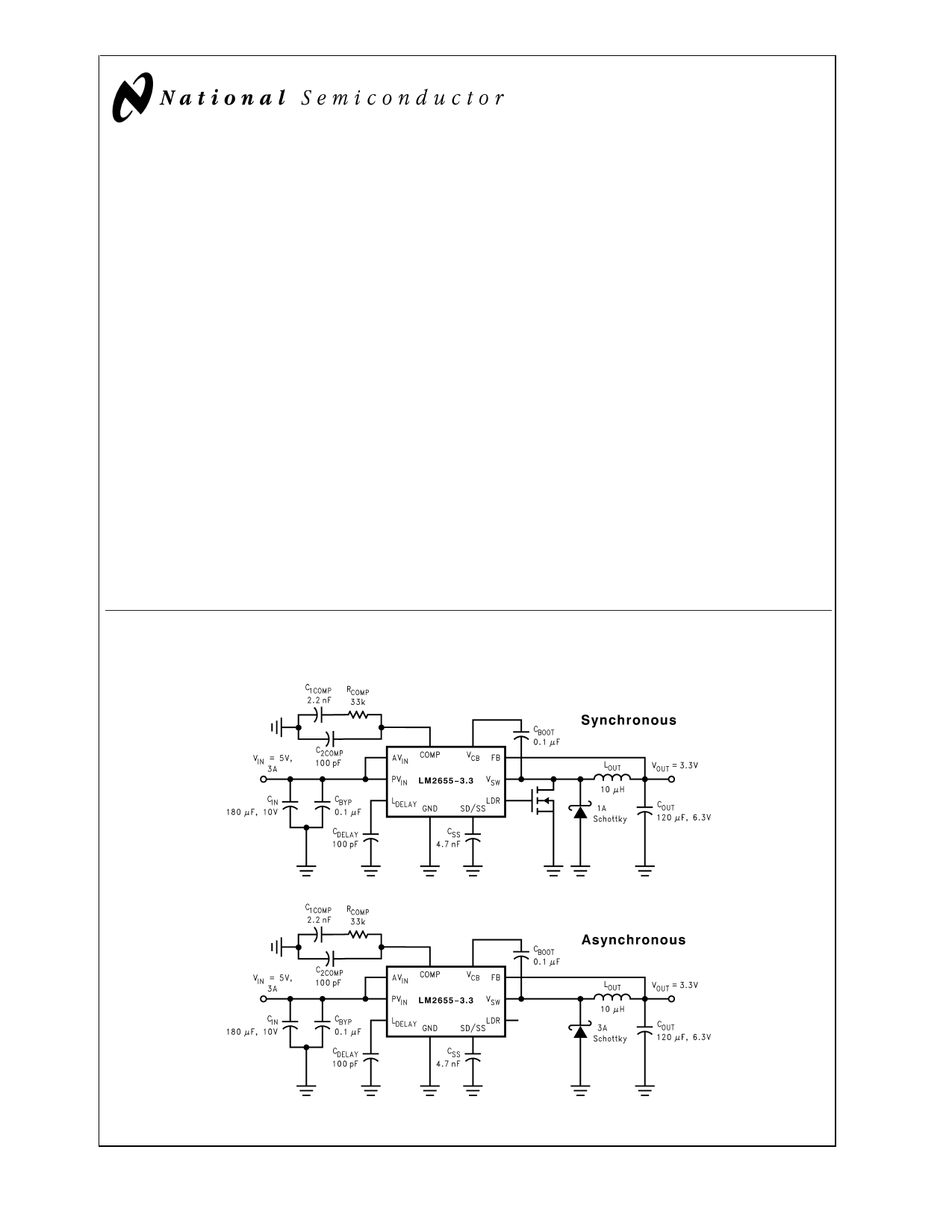
Typical Application
© 2000 National Semiconductor Corporation DS101284
DS101284-29
www.national.com
1 page 
All Output Voltage Versions Electrical Characteristics
Specifications
Range. VIN =
with
10V
standard typeface are for TJ
unless otherwise specified.
=
25˚C,
and
those
in
boldface
type
apply
over
full
Operating
Temperature
Symbol
Parameter
Conditions
Typical
(Note 6)
Limit
(Note 5)
Units
IQ
Quiescent Current
Shutdown Pin Floating (Device On)
1.7
mA
Device Not Switching
3 mA(max)
IQSD
Quiescent Current in
Shutdown Mode
Shutdown Pin Pulled Low
7 µA
12/20
µA(max)
RDS(ON)
Switch ON Resistance
ISWITCH = 1.5A
33 mΩ
80 mΩ(max)
RSW(ON)
Switch On Resistance
(MOSFET ON Resistance
+ Bonding Wire
Resistance)
ISWITCH = 1.5A
72 mΩ
IL
VBOOT
Switch Leakage Current
Bootstrap Regulator
Voltage
IBOOT = 1 mA
CBOOT=tbd
5 nA
6.7 V
6.4 V(min)
7.0 V(max)
GM Error Amplifier
Transconductance
1250
µmho
AV Error Amplifier Voltage
Gain
100
IEA_SOURCE
Error Amplifier Source
VIN = 4V, VFB = .9*VOUT, VCOMP =
40
µA
Current
2V
32/10
µA(min)
IEA_SINK
Error Amplifier Sink Current VIN = 4V, VFB = 1.1*VOUT, VCOMP =
2V
80
53/30
µA
µA(min)
VEAH
Error Amplifier Output
Swing Upper Limit
VIN = 4V, VFB = .9*VOUT, VCOMP =
2V
2.70 V
2.50/2.40
V(min)
VEAL
Error Amplifier Output
Swing Lower Limit
VIN = 4V, VFB = .9*VOUT, VCOMP =
2V
1.25 V
1.35/1.50
V(max)
FOSC
Oscillator Frequency
Measured at Switch Pin
VIN = 4V
300 kHz
280/255
kHz(min)
330/345
kHz(max)
DMAX
Maximum Duty Cycle
VIN = 4V
95 %
92 %(min)
ISS
Soft-Start Current
Voltage at the SS Pin = 1.4V
11
µA
14 µA(max)
VOUTUV
VOUTOV
ILDELAY__
SOURCE
VOUT Undervoltage
Lockout Threshold Voltage
Hysteresis for VOUTUV
VOUT Overvoltage Lockout
Threshold Voltage
Hysteresis for VOUTOV
LDELAY Pin Source
Current
81 %VOUT
76 %VOUT(min)
84 %VOUT(max)
5 %VOUT
108 %VOUT
106 %VOUT(min)
114 %VOUT(max)
5 %VOUT
5 µA
ISHUTDOWN
Shutdown Pin Current
Shutdown Pin Pulled Low
2.2 µA
3.7/4.0
µA(max)
VSHUTDOWN
Shutdown Pin Threshold
Voltage
Rising Edge
0.6 V
0.25 V(min)
0.9 V(max)
TSD Thermal Shutdown
Temperature
165 ˚C
TSD_HYST
Thermal Shutdown
Hysteresis Temperature
25 ˚C
5 www.national.com
5 Page 
DESIGN PROCEDURE (Continued)
SOFT-START CAPACITOR
A soft-start capacitor is used to provide the soft-start feature.
When the input voltage is first applied, or when the SD(SS)
pin is allowed to go high, the soft-start capacitor is charged
by a current source (approximately 2 µA). When the SD(SS)
pin voltage reaches 0.6V (shutdown threshold), the internal
regulator circuitry starts to operate. The current charging the
soft-start capacitor increases from 2 µA to approximately
10 µA. With the SD(SS) pin voltage between 0.6V and 1.3V,
the level of the current limit is zero, which means the output
voltage is still zero. When the SD(SS) pin voltage increases
beyond 1.3V, the current limit starts to increase. The switch
duty cycle, which is controlled by the level of the current limit,
starts with narrow pulses and gradually gets wider. At the
same time, the output voltage of the converter increases to-
wards the nominal value, which brings down the output volt-
age of the error amplifier. When the output of the error ampli-
fier is less than the current limit voltage, it takes over the
control of the duty cycle. The converter enters the normal
current-mode PWM operation. The SD(SS) pin voltage is
eventually charged up to about 2V.
The soft-start time can be estimated as:
TSS = CSS * 0.6V/2 µA + CSS * (2V−0.6V)/10 µA
During start-up, the internal circuit is monitoring the soft-start
voltage. When the softstart voltage reaches 2V, the under-
voltage and overvoltage protections are enabled.
If the output voltage doesn’t rise above 80% of the normal
value before the soft-start reaches 2V, undervoltage protec-
tion shut down the device. You can avoid this by either in-
creasing the value of the soft-start capacitor, or using a LDE-
LAY capacitor.
LDELAY CAPACITOR
The LDELAY capacitor (CDELAY) provides a means to con-
trol undervoltage latch protection. By changing CDELAY, the
user can adjust the time delay between the output voltage
dropping below 80% of its nominal value and the part shut-
ting off due to undervoltage latch protection. The LDELAY
circuit consists of a 5 µA current source in series with a user
defined capacitor, CDELAY. The 5 µA current source is
turned on whenever the output voltage is below 80% of its
nominal value, otherwise this current source is off. With the
output voltage below 80% of its nominal value, the 5 µA cur-
rent source begins to charge CDELAY, as shown in Figure 2.
If the potential across CDELAY reaches 2V, undervoltage
latch protection will be enabled and the part will shutdown. If
the output voltage recovers to above 80% of its nominal
value before the potential across CDELAY reaches 2V, und-
ervoltage latch protection will remain disabled. Hence, CDE-
LAY sets a time delay by the following equation:
TDELAY (ms) = CDELAY (nF) * 2V/5A
Undervoltage latch protection can be disabled by tying the
LDELAY pin to the ground.
DS101284-22
FIGURE 2. Undervoltage latch protection.
COMPENSATION COMPONENTS
In the control to output transfer function, the first pole Fp1 can
be estimated as 1/(2πROUTCOUT); The ESR zero Fz1 of the
output capacitor is 1/(2πESRCOUT); Also, there is a high fre-
quency pole Fp2 in the range of 45kHz to 150kHz:
Fp2 = Fs/(πn(1−D))
where D = VOUT/VIN, n = 1+0.348L/(VIN−VOUT) (L is in µHs
and VIN and VOUT in volts).
The total loop gain G is approximately 1000/IOUT where IOUT
is in amperes.
A Gm amplifier is used inside the LM2655. The output resis-
tor Ro of the Gm amplifier is about 80kΩ. Cc1 and RC to-
gether with Ro give a lag compensation to roll off the gain:
Fpc1 = 1/(2πCc1(Ro+Rc)), Fzc1 = 1/2πCc1Rc.
In some applications, the ESR zero Fz1 can not be cancelled
by Fp2. Then, Cc2 is needed to introduce Fpc2 to cancel the
ESR zero, Fp2 = 1/(2πCc2Ro\Rc).
The rule of thumb is to have more than 45˚ phase margin at
the crossover frequency (G=1).
If COUT is higher than 68µF, Cc1 = 2.2nF, and Rc = 15KΩ are
good choices for most applications. If the ESR zero is too
low to be cancelled by Fp2, add Cc2.
If the transient response to a step load is important, choose
RC to be higher than 10kΩ.
APPLICATION CIRCUITS
PROGRAMMABLE OUTPUT VOLTAGE
Using the adjustable output version of the LM2655 as shown
in Figure 3, output voltages between 1.24V and 13V can be
achieved. Use the following formula to select the appropriate
resistor values:
RFB1 = RFB2*(VOUT - VREF)/VREF
where VREF = 1.238V.
Select resistors between 10kΩ and 100kΩ. (1% or higher ac-
curacy metal film resistors for RFB1 and RFB2.)
11 www.national.com
11 Page | ||
| Páginas | Total 16 Páginas | |
| PDF Descargar | [ Datasheet LM2655.PDF ] | |
Hoja de datos destacado
| Número de pieza | Descripción | Fabricantes |
| LM2650 | Synchronous Step-Down DC/DC Converter | National Semiconductor |
| LM2650 | LM2650 Synchronous Step-Down DC/DC Converter (Rev. C) | Texas Instruments |
| LM2650M-ADJ | Synchronous Step-Down DC/DC Converter | National Semiconductor |
| LM2651 | 1.5A High Efficiency Synchronous Switching Regulator | National Semiconductor |
| Número de pieza | Descripción | Fabricantes |
| SLA6805M | High Voltage 3 phase Motor Driver IC. |
Sanken |
| SDC1742 | 12- and 14-Bit Hybrid Synchro / Resolver-to-Digital Converters. |
Analog Devices |
|
DataSheet.es es una pagina web que funciona como un repositorio de manuales o hoja de datos de muchos de los productos más populares, |
| DataSheet.es | 2020 | Privacy Policy | Contacto | Buscar |