|
|
|
PDF LM2641 Data sheet ( Hoja de datos )
| Número de pieza | LM2641 | |
| Descripción | Dual Adjustable Step-Down Switching Power Supply Controller | |
| Fabricantes | National Semiconductor | |
| Logotipo | ||
Hay una vista previa y un enlace de descarga de LM2641 (archivo pdf) en la parte inferior de esta página. Total 18 Páginas | ||
|
No Preview Available !
January 2000
LM2641
Dual Adjustable Step-Down Switching Power Supply
Controller
General Description
The LM2641 is a dual step-down power supply controller in-
tended for application in notebook personal computers and
other battery-powered equipment.
Fixed-frequency synchronous drive of logic-level N-channel
power MOSFETs is combined with an optional
pulse-skipping mode to achieve ultra efficient power conver-
sion over a 1000:1 load current range. The pulse-skipping
mode can be disabled in favor of fixed-frequency operation
regardless of the load current level.
High DC gain and current-mode feedback control assure ex-
cellent line and load regulation and a wide loop bandwidth
for fast response to dynamic loads.
An internal oscillator fixes the switching frequency at
300 kHz. Optionally, switching can be synchronized to an ex-
ternal clock running as fast as 400 kHz.
An optional soft-start feature limits current surges from the
input power supply at start up and provides a simple means
of start-up sequencing.
Logic-level inputs allow the controllers to be turned ON and
OFF separately.
Key Specifications
n 96% efficient
n 5.5 to 30V input range
n Dual outputs adjustable from 2.2 to 8V
n 0.5% typical load regulation error
n 0.002%/V typical line regulation error
Features
n 300 kHz fixed-frequency switching
n Switching synchronization with an external signal up to
400 kHz
n Optional pulse-skipping mode
n Adjustable secondary feedback
n Input undervoltage lockout
n Output undervoltage shutdown protection
n Output overvoltage shutdown protection
n Programmable soft-start (each controller)
n 5V, 50 mA linear regulator output
n Precision 2.5V reference output
n 28-pin TSSOP
Applications
n Notebook and subnotebook computers
n Wireless data terminals
n Battery-powered instruments
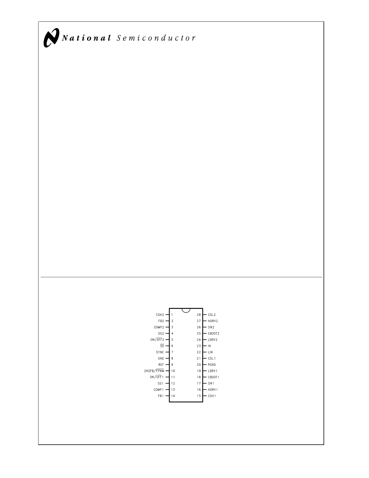
Connection Diagram and Ordering Information
28-Lead TSSOP (MTC)
DS100949-1
Top View
Order Number LM2641MTC-ADJ
See NS Package Number MTC28
© 2000 National Semiconductor Corporation DS100949
www.national.com
1 page 
Absolute Maximum Ratings (Notes 2, 1)
If Military/Aerospace specified devices are required,
please contact the National Semiconductor Sales Office/
Distributors for availability and specifications.
IN, SW1, and SW2
FB1 and FB2
SD, ON/OFF1, ON/OFF2,
2NDFB/FPWM, SYNC, REF,
SS1, SS2, COMP1,
COMP2 and CSL1
LIN
CSH1, CSH2, and CSL2 (Note
12)
Voltage from CBOOT1 to SW1
and from CBOOT2 to SW2
Voltage from HDRV1 to SW1
and from HDRV2 to SW2
−0.3 to 31V
−0.3 to 3V
−0.3 to (VLIN +0.3)V
−0.3 to 6V
−0.3 to 9V
−0.3 to 5V
−0.3V
Voltage from CBOOT1 to
HDRV1 and from CBOOT2
HDRV2
Junction Temp.
Power Dissipation (Note 3)
Ambient Storage Temp. (TJ)
Soldering Dwell Time, Temp. (Note 4)
Wave
Infrared
Vapor Phase
ESD Rating (Note 5)
−0.3V
+150˚C
883 mW
−65 to +150˚C
4 sec, 260˚C
10 sec, 240˚C
75 sec, 219˚C
2 kV
Operating Ratings (Notes 1, 2)
VIN
Junction Temp. (TJ)
5.5 to 30V
0 to +125˚C
Electrical Characteristics
Typicals and limits appearing in regular type apply for TJ = 25˚C. Limits appearing in boldface type apply over the entire junc-
tion temperature
= 10V, and VSD
range for operation, 0 to +125˚C. Unless otherwise
= VON/OFF1 = VON/OFF2 = 5V. (Notes 2, 6, 7)
specified
under
the
Parameter
or
Conditions
columns,
VIN
Symbol
Parameter
Conditions
Typical
Limit
Units
System
VIN Input Supply Voltage Range
5.5 V(min)
30 V(max)
VOUT1
Output Voltage Adjustment
Range
2.2 V(min)
6.0 V(max)
VOUT2
Output Voltage Adjustment
Range
2.2 V(min)
8.0 V(max)
∆VOUT/VOUT
Load Regulation
0 mV ≤ (CSH1-CSL1) ≤ 80 mV,
0 mV ≤ (CSH2-CSL2) ≤ 80 mV
0.5
%
∆VOUT/∆VIN
IIN
Line Regulation
Input Supply Current
5.5V ≤ VIN ≤ 30V
ON (Note 8)
VFB1 = VFB2 = 1.4V,
VCSH1 = 5.2V, VCSL1 = 5V,
VCSH2 = 3.5V, VCSL2 = 3.3V
Standing By (Note 9)
0.002
0.6
80
%/V
mA
1 mA(max)
µA
VON/OFF1 = VON/OFF2 = 0V
Shut Down (Note 10)
150 µA(max)
25 µA
ISS1, ISS2
Soft-Start Source Current
VSD = 0V
VSS1 = VSS2 = 1V
60 µA(max)
4.75 µA
2.0 µA(min)
7.0 µA(max)
Soft-Start Sink Current
10 µA
VPCL
Positive Current Limit
Voltage (Voltage from CSH1
to CSL1 and from CSH2 to
CSL2)
100 mV
80 mV(min)
140 mV(max)
VNCL
Negative Current Limit
Voltage (Voltage from CSH1
to CSL1 and from CSH2 to
CSL2)
V2NDFB/FPWM = 0.8V
−100
−80
−140
mV
mV(min)
mV(max)
5 www.national.com
5 Page 
Theory of Operation (Continued)
losses. The load current value where the transition from
fixed-frequency to pulse-skipping operation occurs is the
point where the inductor current goes low enough to cause
the voltage measured across the current sense resistor (R4
or R13) to drop below 25 mV.
In pulse-skipping mode, the high-side FET switch will turn
ON at the beginning of the first clock cycle which occurs after
the voltage at the feedback pin falls below the reference volt-
age. The high-side FET switch remains ON until the voltage
across the current sense resistor rises to 25 mV (and then it
turns OFF).
Ramp Compensation
All current-mode controllers require the use of ramp com-
pensation to prevent subharmonic oscillations, and this com-
pensation is built into the LM2641. The internal compensa-
tion assumes an RSENSE value of 25 mΩ, inductor value of
6.8µH, and a maximum output voltage of 6V.
To prevent oscillations, the slope M of the compensation
ramp must be equal to the maximum downward slope of the
voltage waveform at the output of the current sense ampli-
fier. The relationship of the slope M to the external compo-
nents is given by:
MCOMP = MCS AMP (max) = N X RSENSE X VOUT (max) / L
Where:
MCOMP is the slope of the compensation ramp.
MCS AMP (max) is the maximum downward slope of the volt-
age at the output of the current sense amplifier.
N is the gain of the current sense amplifier.
RSENSE is the value of the current sense resistor.
VOUT (max) is the maximum output voltage.
L is the inductance of the output inductor.
It is important to note that since the value RSENSE appears in
the numerator and L is in the denominator, these two values
may be increased or decreased at the same ratio without
changing the slope.
At higher values of load current, a lower value RSENSE will be
selected. The inductance value for the output inductor
should be decreased by the same percentage to maintain
correct ramp compensation.
Application Information
Improved Transient Response
If the output voltage falls below 97% of the nominal value,
the low-voltage regulation (LREG) comparator will activate
logic which turns ON the high-side FET switch continuously
until the output returns to nominal. The low-side FET switch
is held OFF during this time.
This action will improve transient response since it bypasses
the error amplifier and PWM comparator, forcing the
high-side switch ON until the output returns to nominal. This
feature is disabled during start-up.
Boost High-Side Gate Drive
A “flying” bootstrap capacitor is used to generate the gate
drive voltage used for the high-side FET switch. This boot-
strap capacitor is charged up to about 5V using an internal
supply rail and diode when ever the low-side FET switch is
ON. When the high-side FET switch turns ON, the Source is
pulled up near the input voltage. The voltage across the
bootstrap capacitor boosts up the gate drive voltage, ensur-
ing that the Gate is driven at least 4.3V higher than the
Source.
Reference
The internal bandgap reference is used to generate a 2.5V
reference voltage which is connected to the REF pin. The
guaranteed tolerance of the REF voltage is ±2% over the full
operating temperature range, as long as the current drawn is
≤ 5 mA.
A bypass capacitor on the REF pin is not required, but may
be used to reduce noise.
5V LIN Output
The LM2641 contains a built-in 5V/50 mA LDO regulator
whose output is connected to the LIN pin. Since this is an
LDO regulator, it does require an external capacitor to main-
tain stability. A good quality Tantalum capacitor ≥ 4.7µF is
recommended.
Since the current limit for this LDO regulator is set at about
85 mA, it can be used at load currents up to about 50 mA
(assuming total IC power dissipation does not exceed the
maximum value).
Guaranteed specifications are provided for worst-case val-
ues of VLIN over the full operating temperature range for load
currents up to 25mA (see Electrical Characteristics). To esti-
mate how the VLIN output voltage changes when going from
ILIN = 25mA to ILIN = 50mA, a change in VLIN of about
−30mV should be expected due to loading (typical value
only, not guaranteed). This decrease in VLIN is linear with in-
creasing load current.
It must be understood that the maximum allowable current of
50mA must include the current drawn by the gate drive cir-
cuitry. This means that the maximum current available for
use at the LIN pin is 50 mA minus whatever is being used in-
ternally for gate drive.
The amount of current used for gate drive by each switching
output can be calculated using the formula:
Where:
IGD = 2 X Q X FOSC
IGD is the gate drive current supplied by VLIN.
Q is the gate charge required by the selected FET (see FET
data sheet: Gate Charge Characteristics).
FOSC is the switching frequency.
Example: As shown in the typical application, if the FET
NDS8410 is used with the LM2641, the turn-on gate voltage
(VGS) is 5V − VDIODE = 4.3V. Referring to the NDS8410 data
sheet, the curve Gate Charge Characteristics shows that the
gate charge for this value of VGS is about 24 nC.
Assuming 300 kHz switching frequency, the gate drive cur-
rent used by each switching output is:
IGD = 2 X Q X FOSC
= 2 X (24 X 10−9) X (3 X 105)
= 14.4 mA
If both outputs are switching, the total gate drive current
drawn would be twice (28.8 mA).
Note that in cases where the voltage at switching output #1
is 4.8V or higher, the internal gate drive current is obtained
from that output (which means the full 50 mA is available for
external use at the LIN pin).
11 www.national.com
11 Page | ||
| Páginas | Total 18 Páginas | |
| PDF Descargar | [ Datasheet LM2641.PDF ] | |
Hoja de datos destacado
| Número de pieza | Descripción | Fabricantes |
| LM2640 | Dual Adjustable Step-Down Switching Power Supply Controller | National Semiconductor |
| LM2640 | LM2640 Dual Adjustable Step-Down Switching Power Supply Controller (Rev. B) | Texas Instruments |
| LM26400Y | LM26400Y Dual 2-A 500-kHz Wide Input Range Buck Regulator (Rev. D) | Texas Instruments |
| LM26400Y | 500kHz Wide Input Range Buck Regulator | National Semiconductor |
| Número de pieza | Descripción | Fabricantes |
| SLA6805M | High Voltage 3 phase Motor Driver IC. |
Sanken |
| SDC1742 | 12- and 14-Bit Hybrid Synchro / Resolver-to-Digital Converters. |
Analog Devices |
|
DataSheet.es es una pagina web que funciona como un repositorio de manuales o hoja de datos de muchos de los productos más populares, |
| DataSheet.es | 2020 | Privacy Policy | Contacto | Buscar |