|
|
PDF 28J60 Data sheet ( Hoja de datos )
| Número de pieza | 28J60 | |
| Descripción | ENC28J60 | |
| Fabricantes | Microchip Technology | |
| Logotipo |  |
|
Hay una vista previa y un enlace de descarga de 28J60 (archivo pdf) en la parte inferior de esta página. Total 30 Páginas | ||
|
No Preview Available !
www.DataSheet4U.com
ENC28J60
Data Sheet
Stand-Alone Ethernet Controller
with SPI Interface
© 2006 Microchip Technology Inc.
Preliminary
DS39662B
1 page 
ENC28J60
1.0 OVERVIEW
The ENC28J60 is a stand-alone Ethernet controller
with an industry standard Serial Peripheral Interface
(SPI). It is designed to serve as an Ethernet network
interface for any controller equipped with SPI.
The ENC28J60 meets all of the IEEE 802.3 specifica-
tions. It incorporates a number of packet filtering
schemes to limit incoming packets. It also provides an
internal DMA module for fast data throughput and hard-
ware assisted checksum calculation, which is used in
various network protocols. Communication with the
host controller is implemented via an interrupt pin and
the SPI, with clock rates of up to 20 MHz. Two dedi-
www.DataSheet4U.comcated pins are used for LED link and network activity
indication.
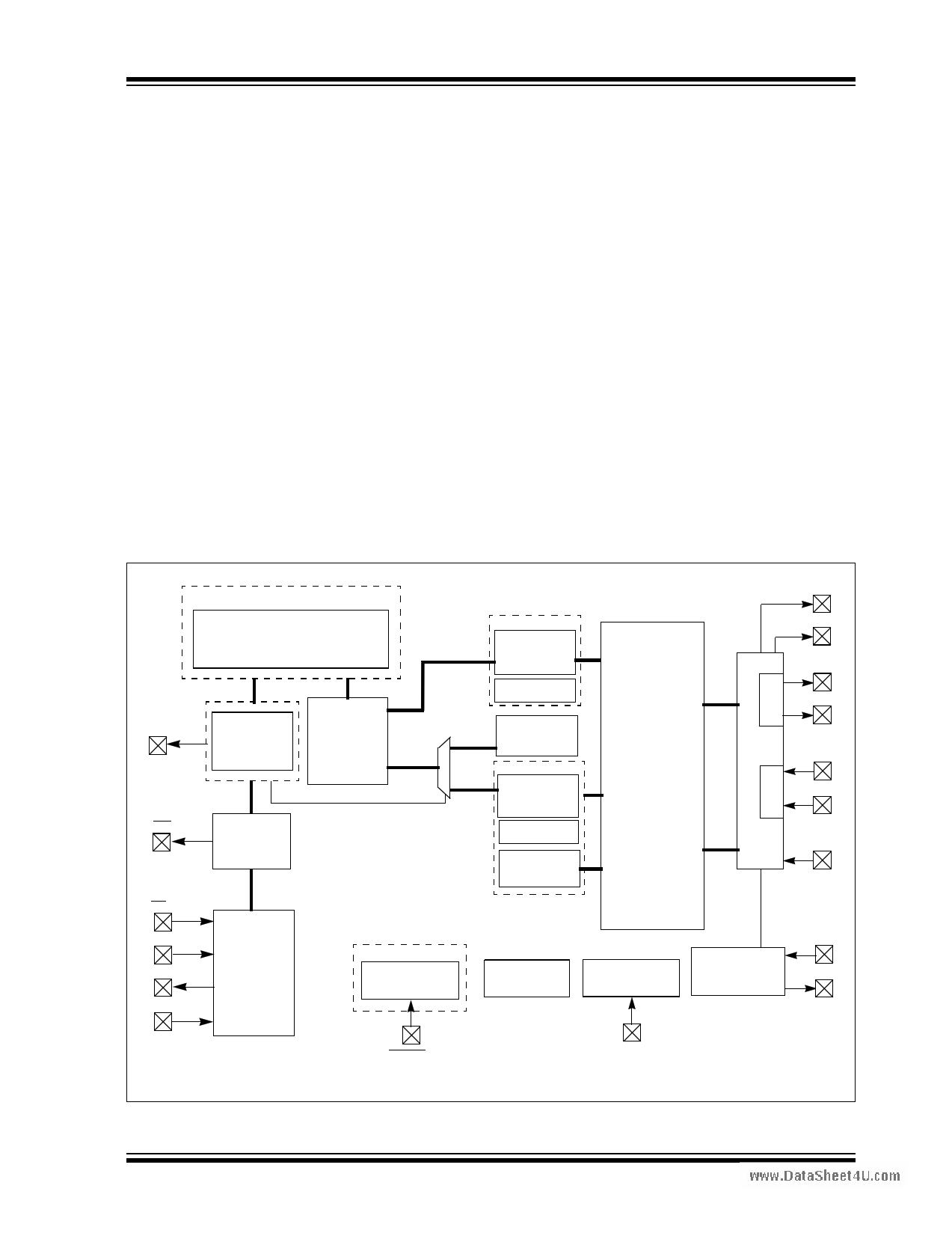
A simple block diagram of the ENC28J60 is shown in
Figure 1-1. A typical application circuit using the device
is shown in Figure 1-2. With the ENC28J60, two pulse
transformers and a few passive components are all that
is required to connect a microcontroller to an Ethernet
network.
The ENC28J60 consists of seven major functional
blocks:
1. An SPI interface that serves as a communica-
tion channel between the host controller and the
ENC28J60.
2. Control Registers which are used to control and
monitor the ENC28J60.
3. A dual port RAM buffer for received and
transmitted data packets.
4. An arbiter to control the access to the RAM
buffer when requests are made from DMA,
transmit and receive blocks.
5. The bus interface that interprets data and
commands received via the SPI interface.
6. The MAC (Medium Access Control) module that
implements IEEE 802.3 compliant MAC logic.
7. The PHY (Physical Layer) module that encodes
and decodes the analog data that is present on
the twisted pair interface.
The device also contains other support blocks, such as
the oscillator, on-chip voltage regulator, level translators
to provide 5V tolerant I/Os and system control logic.
FIGURE 1-1:
ENC28J60 BLOCK DIAGRAM
Buffer
8 Kbytes
Dual Port RAM
CLKOUT
Control
Registers
ch0
Arbiter
ch1
INT
Bus Interface
RX
RXBM
RXF (Filter)
DMA &
ch0 Checksum
TX
ch1
TXBM
Flow Control
Host Interface
MAC
MII
Interface
MIIM
Interface
LEDA
LEDB
TPOUT+
TX TPOUT-
PHY
TPIN+
RX TPIN-
RBIAS
CS(1)
SI(1)
SO
SCK(1)
SPI
System Control
Power-on
Reset
Voltage
Regulator
25 MHz
Oscillator
OSC1
OSC2
Note 1: These pins are 5V tolerant.
RESET(1)
VCAP
© 2006 Microchip Technology Inc.
Preliminary
DS39662B-page 3
5 Page 
ENC28J60
REGISTER 2-2: PHLCON: PHY MODULE LED CONTROL REGISTER
R/W-0
r
bit 15
R/W-0
r
R/W-1
r
R/W-1
r
R/W-0
LACFG3
R/W-1
LACFG2
R/W-0
LACFG1
R/W-0
LACFG0
bit 8
R/W-0
LBCFG3
bit 7
R/W-0
LBCFG2
R/W-1
LBCFG1
R/W-0
LBCFG0
R/W-0
LFRQ1
R/W-0
LFRQ0
R/W-1
STRCH
R/W-x
r
bit 0
Legend:
R = Readable bit
-n = Value at POR
www.DataSheet4U.com
W = Writable bit
‘1’ = Bit is set
U = Unimplemented bit, read as ‘0’
‘0’ = Bit is cleared
x = Bit is unknown
bit 15-14
bit 13-12
bit 11-8
bit 7-4
bit 3-2
bit 1
bit 0
Reserved: Write as ‘0’
Reserved: Write as ‘1’
LACFG3:LACFG0: LEDA Configuration bits
1111 = Reserved
1110 = Display duplex status and collision activity (always stretched)
1101 = Display link status and transmit/receive activity (always stretched)
1100 = Display link status and receive activity (always stretched)
1011 = Blink slow
1010 = Blink fast
1001 = Off
1000 = On
0111 = Display transmit and receive activity (stretchable)
0110 = Reserved
0101 = Display duplex status
0100 = Display link status
0011 = Display collision activity (stretchable)
0010 = Display receive activity (stretchable)
0001 = Display transmit activity (stretchable)
0000 = Reserved
LBCFG3:LBCFG0: LEDB Configuration bits
1110 = Display duplex status and collision activity (always stretched)
1101 = Display link status and transmit/receive activity (always stretched)
1100 = Display link status and receive activity (always stretched)
1011 = Blink slow
1010 = Blink fast
1001 = Off
1000 = On
0111 = Display transmit and receive activity (stretchable)
0110 = Reserved
0101 = Display duplex status
0100 = Display link status
0011 = Display collision activity (stretchable)
0010 = Display receive activity (stretchable)
0001 = Display transmit activity (stretchable)
0000 = Reserved
LFRQ1:LFRQ0: LED Pulse Stretch Time Configuration bits (see Table 2-1)
11 = Reserved
10 = Stretch LED events by TLSTRCH
01 = Stretch LED events by TMSTRCH
00 = Stretch LED events by TNSTRCH
STRCH: LED Pulse Stretching Enable bit
1 = Stretchable LED events will cause lengthened LED pulses based on LFRQ1:LFRQ0 configuration
0 = Stretchable LED events will only be displayed while they are occurring
Reserved: Write as ‘0’
© 2006 Microchip Technology Inc.
Preliminary
DS39662B-page 9
11 Page | ||
| Páginas | Total 30 Páginas | |
| PDF Descargar | [ Datasheet 28J60.PDF ] | |
Hoja de datos destacado
| Número de pieza | Descripción | Fabricantes |
| 28J60 | ENC28J60 | Microchip Technology |
| Número de pieza | Descripción | Fabricantes |
| SLA6805M | High Voltage 3 phase Motor Driver IC. |
Sanken |
| SDC1742 | 12- and 14-Bit Hybrid Synchro / Resolver-to-Digital Converters. |
Analog Devices |
|
DataSheet.es es una pagina web que funciona como un repositorio de manuales o hoja de datos de muchos de los productos más populares, |
| DataSheet.es | 2020 | Privacy Policy | Contacto | Buscar |
