|
|
PDF 80286 Data sheet ( Hoja de datos )
| Número de pieza | 80286 | |
| Descripción | Hihj Performance Microprocessor | |
| Fabricantes | intersil | |
| Logotipo |  |
|
Hay una vista previa y un enlace de descarga de 80286 (archivo pdf) en la parte inferior de esta página. Total 13 Páginas | ||
|
No Preview Available !
www.DataSheet4U.com
TM
80C286/883
March 1997
High Performance Microprocessor with Memory
Management and Protection
Features
Description
• This Circuit is Processed in Accordance to MIL-STD-
883 and is Fully Conformant Under the Provisions of
Paragraph 1.2.1.
• Compatible with NMOS 80286/883
• Static CMOS Design for Low Power Operation
- ICCSB = 5mA Maximum
- ICCOP = 185mA Maximum (80C286-10/883)
- ICCOP = 220mA Maximum (80C286-12/883)
• Large Address Space
- 16 Megabytes Physical
- 1 Gigabyte Virtual per Task
• Integrated Memory Management, Four-Level Memory
Protection and Support for Virtual Memory and
Operating Systems
• Two 80C86 Upward Compatible Operating Modes
- 80C286/883 Real Address Mode
- Protected Virtual Address Mode
• Compatible with 80287 Numeric Data Co-Processor
The Intersil 80C286/883 is a static CMOS version of the
NMOS 80286 microprocessor. The 80C286/883 is an
advanced, high-performance microprocessor with specially
optimized capabilities for multiple user and multi-tasking sys-
tems. The 80C286/883 has built-in memory protection that
supports operating system and task isolation as well as pro-
gram and data privacy within tasks. The 80C286/883
includes memory management capabilities that map 230
(one gigabyte) of virtual address space per task into 224
bytes (16 megabytes) of physical memory.
The 80C286/883 is upwardly compatible with 80C86 and
80C88 software (the 80C286/883 instruction set is a super-
set of the 80C86/80C88 instruction set). Using the 80C286/
883 real address mode, the 80C286/883 is object code com-
patible with existing 80C86 and 80C88 software. In pro-
tected virtual address mode, the 80C286/883 is source code
compatible with 80C86 and 80C88 software but may require
upgrading to use virtual address as supported by the
80C286/883’s integrated memory management and protec-
tion mechanism. Both modes operate at full 80C286/883
performance and execute a superset of the 80C86 and
80C88 instructions.
The 80C286/883 provides special operations to support the
efficient implementation and execution of operating systems.
For example, one instruction can end execution of one task,
save its state, switch to a new task, load its state, and start
execution of the new task. The segment-not-present excep-
tion and restartable instructions.
Ordering Information
PACKAGE TEMP. RANGE
10MHz
12.5MHz
16MHz
68 Pin PGA
0oC to +70oC
-
CG80C286-12
CG80C286-16
-40oC to +85oC IG80C286-10
IG80C286-12
-
-55oC to +125oC MG80C286-10/883 MG80C286-12/883
-
5962-9067801MXC 5962-9067802MXC
-
20MHz
CG80C286-20
-
-
-
25MHz PKG. NO.
- G68.B
- G68.B
- G68.B
- G68.B
CAUTION: These devices are sensitive to electrostatic discharge; follow proper IC Handling Procedures.
1-888-INTERSIL or 321-724-7143 | Intersil (and design) is a trademark of Intersil Americas Inc.
Copyright © Intersil Americas Inc. 2002. All Rights Reserved
128
FN2948.1
1 page 
www.DataSheet4U.com
80C286/883
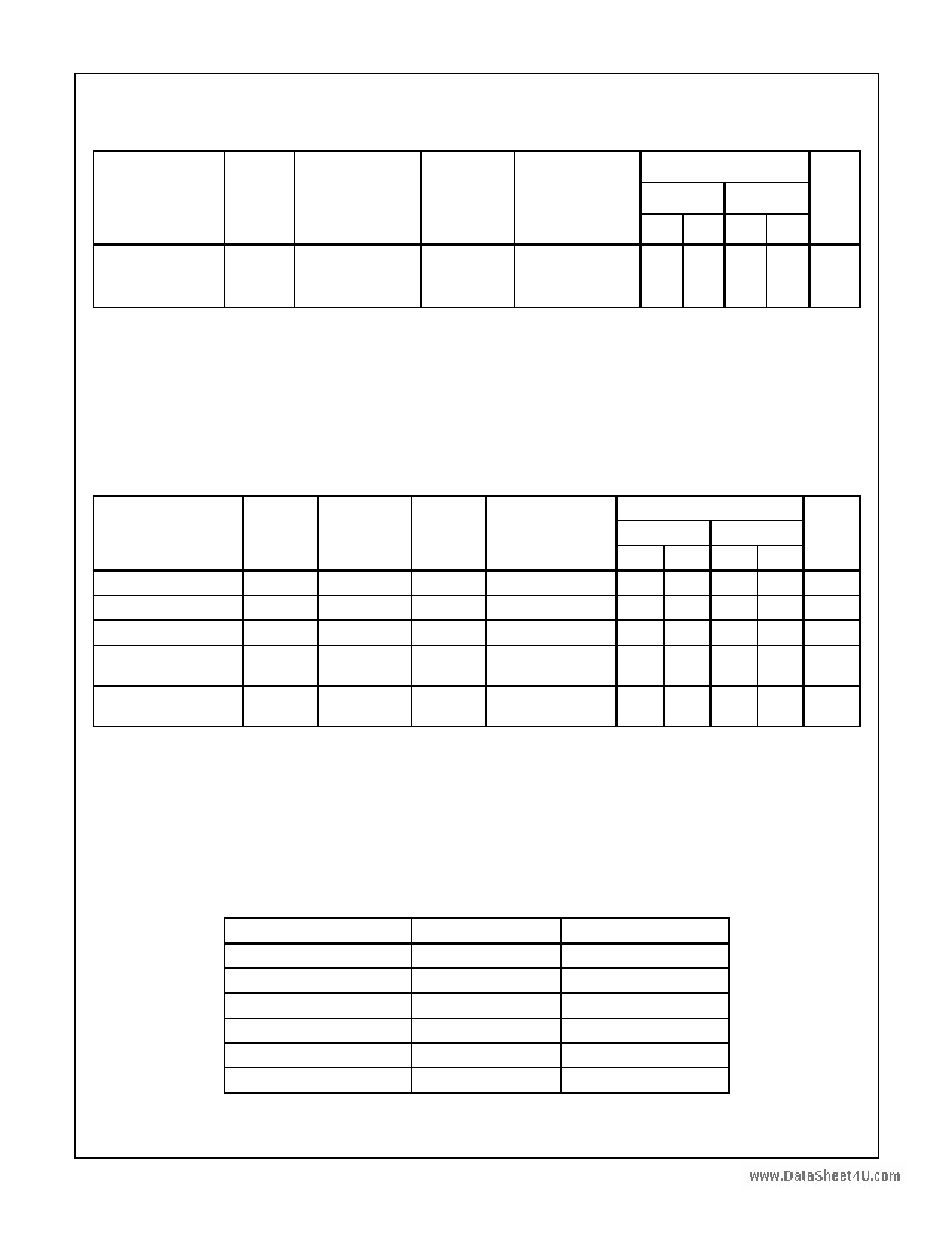
TABLE 2. 80C286/883 AC ELECTRICAL PERFORMANCE SPECIFICATIONS (Continued)
AC Timings are Referenced to 0.8V and 2.0V Points of the Signals as Illustrated in Datasheet Waveforms, Unless Otherwise Noted. Device
Guaranteed and 100% Tested.
80C286/883
PARAMETER
HLDA Valid Delay
(Note 5)
SYMBOL
CONDITIONS
15 VCC = 4.5V and
5.5V, CL = 100pF
IL = |2mA|
GROUP A
SUBGROUPS TEMPERATURE
10MHz
12.5MHz
MIN MAX MIN MAX UNITS
9, 10, 11
-55oC ≤ TA ≤ +125oC 0
47
0
25
ns
NOTES:
1. Asynchronous inputs are INTR, NMI, HOLD, PEREQ, ERROR, and BUSY. This specification is given only for testing purposes, to assure
recognition at a specific CLK edge.
2. Delay from 1.0V on the CLK to 0.8V or 2.0V.
3. Delay from 1.0V on the CLK to 0.8V for Min (HOLD time) and to 2.0V for Max (inactive delay).
4. Delay from 1.0V on the CLK to 2.0V for Min (HOLD time) and to 0.8V for Max (active delay).
5. Delay from 1.0V on the CLK to 2.0V.
TABLE 3. 80C286/883 ELECTRICAL PERFORMANCE SPECIFICATIONS
80C286/883
10MHz
12.5MHz
PARAMETER
SYMBOL CONDITIONS NOTES
TEMPERATURE MIN MAX MIN MAX UNITS
CLK Input Capacitance
CCLK
FREQ = 1MHz
5
TA = +25oC
- 10 - 10 pF
Other Input Capacitance CIN FREQ = 1MH
5
TA = +25oC
- 10 - 10 pF
I/O Capacitance
CI/O FREQ = 1MH
5
TA = +25oC
- 10 - 10 pF
Address/Status/Data
Float Delay
15
1, 3, 4, 5 -55oC ≤ TA ≤ +125oC 0 47 0 32 ns
Address Valid to Status
SETUP Time
19 IL = | 2.0mA| 1, 2, 5 -55oC ≤ TA ≤ +125oC 27 - 20 -
ns
NOTES:
1. Output Load: CL = 100pF.
2. Delay measured from address either reaching 0.8V or 2.0V (valid) to status going active reaching 0.8V or status going inactive reaching
2.0V.
3. Delay from 1.0V on the CLK to Float (no current drive) condition.
4. IL = -6mA (VOH to Float), IL = 8mA (VOL to Float).
5. The parameters listed in Table 3 are controlled via design or process parameters and are not directly tested. These parameters are char-
acterized upon initial design and after major process and/or design changes.
TABLE 4. APPLICABLE SUBGROUPS
CONFORMANCE GROUPS
METHOD
SUBGROUPS
Initial Test
Interim Test
PDA
100%/5004
100%/5004
100%
-
1, 7, 9
1
Final Test
100%
2, 3, 8A, 8B, 10, 11
Group A
Group C & D
-
Samples/5005
1, 2, 3, 7, 8A, 8B, 9, 10, 11
1, 7, 9
132
5 Page 
www.DataSheet4U.com
80C286/883
Waveforms (Continued)
BUS CYCLE TYPE
VCH
CLK
VCL
HILDA
TH
φ1
φ2
16
TH OR TI
φ1 φ2
TI
φ1
φ2
TH
φ1 φ2
(SEE NOTE 4)
16
S1 • S0
PEACK
BHE, LOCK
A23 - A0,
M/IO,
COD/INTA
D15 - D0
12A (NOTE 3)
12B IF TS
(SEE NOTE 5)
13
IF NPX TRANSFER
VALID
(SEE NOTE 6)
14
15 (SEE NOTE 3)
15
(SEE NOTE 1)
15
(SEE NOTE 2)
15
VALID IF WRITE
PCLK
NOTES:
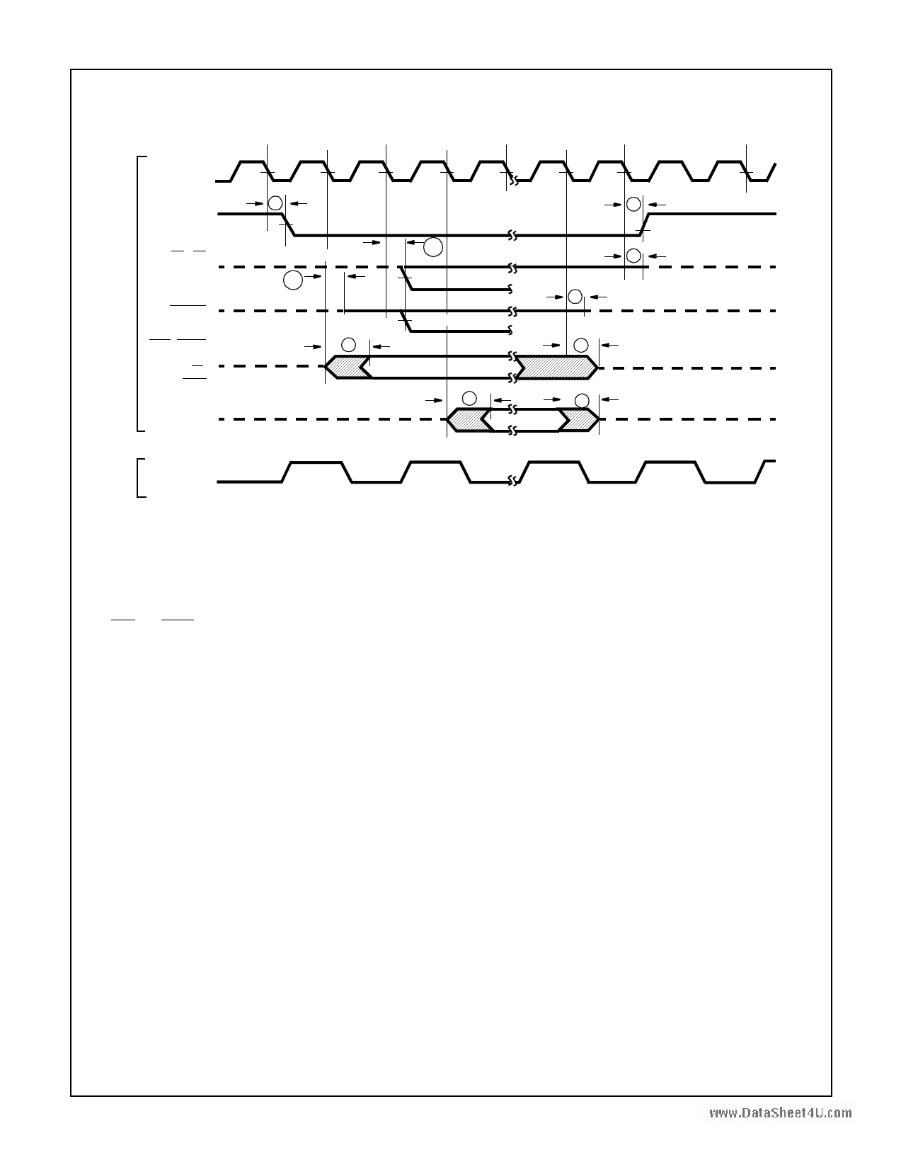
1. These signals may not be driven by the 80C286/883 during the time shown. The worst case in terms of latest float time is shown.
2. The data bus will be driven as shown if the last cycle before TI in the diagram was a write TC.
3. The 80C286/883 puts its status pins in a high impedance logic one state during TH.
4. For HOLD request set up to HLDA, refer to Figure 8.
5. BHE and LOCK are driven at this time but will not become valid until TS.
6. The data bus will remain in a high impedance state if a read cycle is performed.
FIGURE 5. EXITING AND ENTERING HOLD
138
11 Page | ||
| Páginas | Total 13 Páginas | |
| PDF Descargar | [ Datasheet 80286.PDF ] | |
Hoja de datos destacado
| Número de pieza | Descripción | Fabricantes |
| 80286 | Intergrated Optical Disk Controller | Advanced Micro Devices |
| 80286 | Hihj Performance Microprocessor | intersil |
| Número de pieza | Descripción | Fabricantes |
| SLA6805M | High Voltage 3 phase Motor Driver IC. |
Sanken |
| SDC1742 | 12- and 14-Bit Hybrid Synchro / Resolver-to-Digital Converters. |
Analog Devices |
|
DataSheet.es es una pagina web que funciona como un repositorio de manuales o hoja de datos de muchos de los productos más populares, |
| DataSheet.es | 2020 | Privacy Policy | Contacto | Buscar |
