|
|
|
PDF C8051F410 Data sheet ( Hoja de datos )
| Número de pieza | C8051F410 | |
| Descripción | (C8051F410 - C8051F413) 12-bit ADC | |
| Fabricantes | Silicon Laboratories | |
| Logotipo | ||
Hay una vista previa y un enlace de descarga de C8051F410 (archivo pdf) en la parte inferior de esta página. Total 30 Páginas | ||
|
No Preview Available !
www.DataSheet4U.com
C8051F410/1/2/3
2.0 V, 32/16 kB Flash, smaRTClock, 12-bit ADC
Analog Peripherals
- 12-Bit ADC
• ±1 LSB INL; no missing codes
• Programmable throughput up to 200 ksps
• Up to 24 external inputs
• Data dependent windowed interrupt generator
• Built-in temperature sensor (±3 °C)
- Two 12-Bit Current Mode DACs
- Two Comparators
• Programmable hysteresis and response time
• Configurable as wake-up or reset source
- POR/Brownout Detector
- Voltage Reference—1.5, 2.2 V (programmable)
On-Chip Debug
- On-chip debug circuitry facilitates full-speed, non-
intrusive in-system debug (No emulator required)
- Provides breakpoints, single stepping
- Inspect/modify memory and registers
- Complete development kit
Supply Voltage 2.0 to 5.25 V
- Built-in LDO regulator: 2.1 or 2.5 V
High Speed 8051 µC Core
- Pipelined instruction architecture; executes 70% of
instructions in 1 or 2 system clocks
- Up to 50 MIPS throughput with
50 MHz system clock
- Expanded interrupt handler
Memory
- 2304 bytes internal data RAM (256 + 2048)
- 32/16 kB Flash; In-system programmable in
512 byte sectors
- 64 bytes battery-backed RAM (smaRTClock)
Digital Peripherals
- 24 port I/O; push-pull or open-drain, up to 5.25 V
tolerance
- Hardware SMBus™ (I2C™ Compatible), SPI™, and
UART serial ports available concurrently
- Four general purpose 16-bit counter/timers
- Programmable 16-bit counter/timer array with six
capture/compare modules, WDT
- Hardware smaRTClock operates down to 1 V with
64 bytes battery-backed RAM and backup voltage
regulator
Clock Sources
- Internal oscillators: 24.5 MHz 2% accuracy supports
UART operation; clock multiplier up to 50 MHz
- External oscillator: Crystal, RC, C, or Clock
(1 or 2 pin modes)
- smaRTClock oscillator: 32 kHz Crystal or
self-resonant oscillator
- Can switch between clock sources on-the-fly
32-PIN LQFP or 28-PIN 5x5 QFN
Temperature Range: –40 to +85 °C
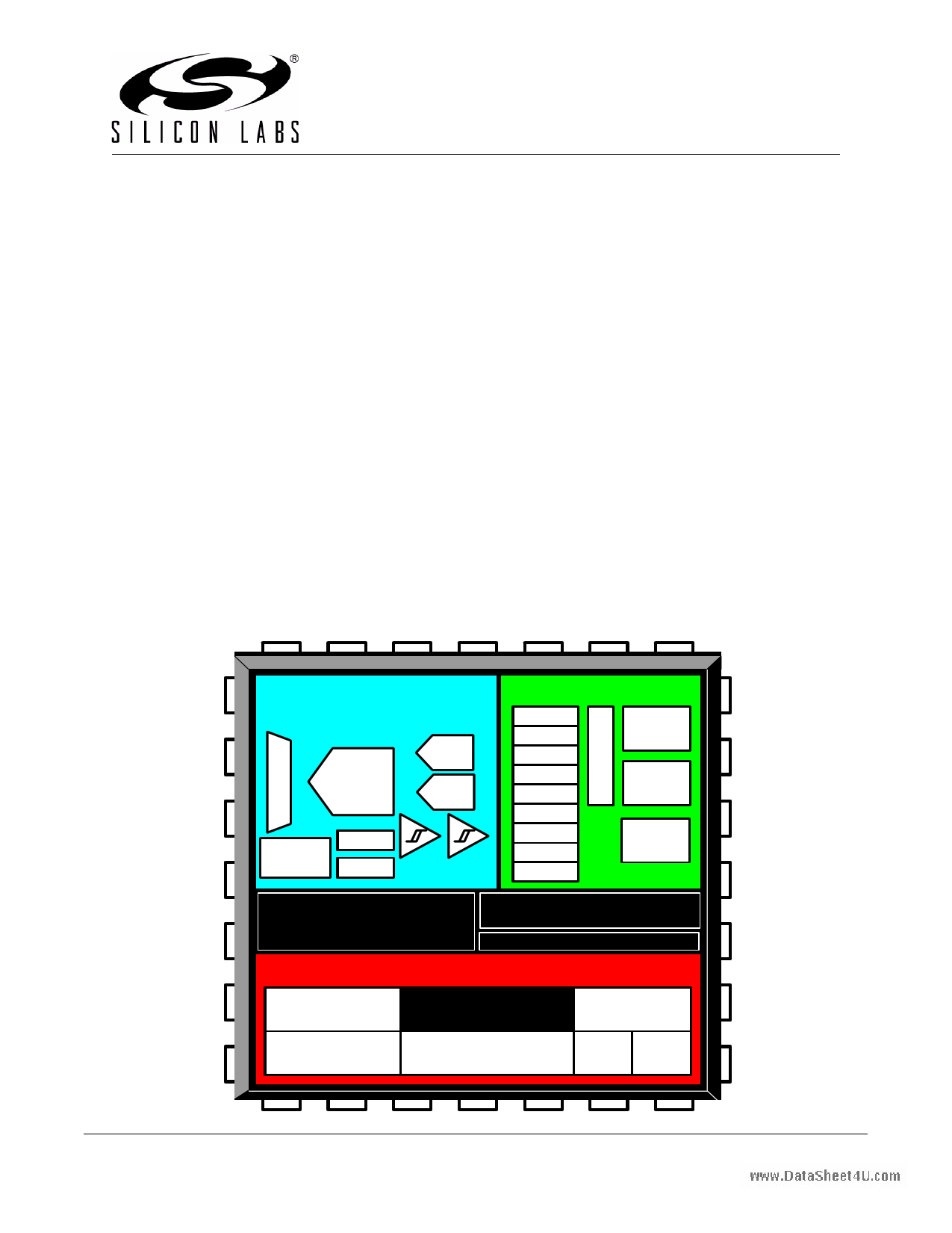
ANALOG
DIGITAL I/O
PERIPHERALS
12-bit
A
12-bit
IDAC
M
U
200ksps
X ADC
12-bit
IDAC
++
TEMP
VREF
-
-
SENSOR VREG VOLTAGE
COMPARATORS
UART
SMBus
SPI
PCA
Timer 0
Timer 1
Timer 2
Timer 3
CRC
Port 0
Port 1
Port 2
24.5 MHz PRECISION
INTERNAL OSCILLATOR
WITH CLOCK MULTIPLIER
LOW FREQUENCY
INTERNAL OSCILLATOR
HARDWARE smaRTClock
HIGH-SPEED CONTROLLER CORE
32/16 kB
ISP FLASH
FLEXIBLE
INTERRUPTS
8051 CPU
(50 MIPS)
DEBUG
CIRCUITRY
2368 B
SRAM
POR WDT
Rev. 0.8 11/06
Copyright © 2006 by Silicon Laboratories
C8051F41x
This information applies to a product under development. Its characteristics and specifications are subject to change without notice.
1 page 
www.DataSheet4U.com
C8051F410/1/2/3
16.3.Security Options ............................................................................................. 137
16.4.Flash Write and Erase Guidelines .................................................................. 139
16.4.1.VDD Maintenance and the VDD Monitor ............................................... 139
16.4.2.16.4.2 PSWE Maintenance .................................................................... 140
16.4.3.System Clock ......................................................................................... 140
16.5.Flash Read Timing ......................................................................................... 142
17. External RAM ........................................................................................................ 145
18. Port Input/Output.................................................................................................. 147
18.1.Priority Crossbar Decoder .............................................................................. 149
18.2.Port I/O Initialization ....................................................................................... 151
18.3.General Purpose Port I/O ............................................................................... 154
19. Oscillators ............................................................................................................. 165
19.1.Programmable Internal Oscillator ................................................................... 165
19.1.1.Internal Oscillator Suspend Mode .......................................................... 166
19.2.External Oscillator Drive Circuit...................................................................... 168
19.2.1.Clocking Timers Directly Through the External Oscillator...................... 168
19.2.2.External Crystal Example....................................................................... 168
19.2.3.External RC Example............................................................................. 170
19.2.4.External Capacitor Example................................................................... 170
19.3.Clock Multiplier ............................................................................................... 172
19.4.System Clock Selection.................................................................................. 174
20. smaRTClock (Real Time Clock)........................................................................... 177
20.1.smaRTClock Interface .................................................................................... 178
20.1.1.smaRTClock Lock and Key Functions ................................................... 178
20.1.2.Using RTC0ADR and RTC0DAT to
Access smaRTClock Internal Registers ................................................. 178
20.1.3.smaRTClock Interface Autoread Feature............................................... 178
20.1.4.RTC0ADR Autoincrement Feature......................................................... 179
20.2.smaRTClock Clocking Sources ...................................................................... 182
20.2.1.Using the smaRTClock Oscillator in Crystal Mode ................................ 182
20.2.2.Using the smaRTClock Oscillator in Self-Oscillate Mode ...................... 182
20.2.3.Automatic Gain Control (Crystal Mode Only) ......................................... 183
20.2.4.smaRTClock Bias Doubling ................................................................... 183
20.2.5.smaRTClock Missing Clock Detector..................................................... 183
20.3.smaRTClock Timer and Alarm Function......................................................... 185
20.3.1.Setting and Reading the smaRTClock Timer Value............................... 185
20.3.2.Setting a smaRTClock Alarm ................................................................. 186
20.4.Backup Regulator and RAM ........................................................................... 187
21. SMBus ................................................................................................................... 191
21.1.Supporting Documents ................................................................................... 192
21.2.SMBus Configuration...................................................................................... 192
21.3.SMBus Operation ........................................................................................... 192
21.3.1.Arbitration............................................................................................... 193
21.3.2.Clock Low Extension.............................................................................. 193
21.3.3.SCL Low Timeout................................................................................... 194
Rev. 0.8
5
5 Page 
www.DataSheet4U.com
C8051F410/1/2/3
23. Enhanced Serial Peripheral Interface (SPI0)
Figure 23.1. SPI Block Diagram ............................................................................. 217
Figure 23.2. Multiple-Master Mode Connection Diagram ....................................... 220
Figure 23.3. 3-Wire Single Master and Slave Mode Connection Diagram ............. 220
Figure 23.4. 4-Wire Single Master and Slave Mode Connection Diagram ............. 220
Figure 23.5. Data/Clock Timing Relationship ......................................................... 222
Figure 23.6. SPI Master Timing (CKPHA = 0)........................................................ 227
Figure 23.7. SPI Master Timing (CKPHA = 1)........................................................ 227
Figure 23.8. SPI Slave Timing (CKPHA = 0).......................................................... 228
Figure 23.9. SPI Slave Timing (CKPHA = 1).......................................................... 228
24. Timers
Figure 24.1. T0 Mode 0 Block Diagram.................................................................. 232
Figure 24.2. T0 Mode 2 Block Diagram.................................................................. 233
Figure 24.3. T0 Mode 3 Block Diagram.................................................................. 234
Figure 24.4. Timer 2 16-Bit Mode Block Diagram .................................................. 239
Figure 24.5. Timer 2 8-Bit Mode Block Diagram .................................................... 240
Figure 24.6. Timer 2 Capture Mode Block Diagram ............................................... 241
Figure 24.7. Timer 3 16-Bit Mode Block Diagram .................................................. 244
Figure 24.8. Timer 3 8-Bit Mode Block Diagram .................................................... 245
Figure 24.9. Timer 3 Capture Mode Block Diagram ............................................... 246
25. Programmable Counter Array (PCA0)
Figure 25.1. PCA Block Diagram............................................................................ 249
Figure 25.2. PCA Counter/Timer Block Diagram.................................................... 250
Figure 25.3. PCA Interrupt Block Diagram ............................................................. 251
Figure 25.4. PCA Capture Mode Diagram.............................................................. 252
Figure 25.5. PCA Software Timer Mode Diagram .................................................. 253
Figure 25.6. PCA High-Speed Output Mode Diagram............................................ 254
Figure 25.7. PCA Frequency Output Mode ............................................................ 255
Figure 25.8. PCA 8-Bit PWM Mode Diagram ......................................................... 256
Figure 25.9. PCA 16-Bit PWM Mode...................................................................... 257
Figure 25.10. PCA Module 5 with Watchdog Timer Enabled ................................. 258
26. C2 Interface
Figure 26.1. Typical C2 Pin Sharing....................................................................... 267
Rev. 0.8
11
11 Page | ||
| Páginas | Total 30 Páginas | |
| PDF Descargar | [ Datasheet C8051F410.PDF ] | |
Hoja de datos destacado
| Número de pieza | Descripción | Fabricantes |
| C8051F410 | (C8051F410 - C8051F413) 12-bit ADC | Silicon Laboratories |
| C8051F411 | (C8051F410 - C8051F413) 12-bit ADC | Silicon Laboratories |
| C8051F412 | (C8051F410 - C8051F413) 12-bit ADC | Silicon Laboratories |
| C8051F413 | (C8051F410 - C8051F413) 12-bit ADC | Silicon Laboratories |
| Número de pieza | Descripción | Fabricantes |
| SLA6805M | High Voltage 3 phase Motor Driver IC. |
Sanken |
| SDC1742 | 12- and 14-Bit Hybrid Synchro / Resolver-to-Digital Converters. |
Analog Devices |
|
DataSheet.es es una pagina web que funciona como un repositorio de manuales o hoja de datos de muchos de los productos más populares, |
| DataSheet.es | 2020 | Privacy Policy | Contacto | Buscar |