|
|
|
PDF TC90A80F Data sheet ( Hoja de datos )
| Número de pieza | TC90A80F | |
| Descripción | 3-Line Digital Comb Filter | |
| Fabricantes | Toshiba Semiconductor | |
| Logotipo | ||
Hay una vista previa y un enlace de descarga de TC90A80F (archivo pdf) en la parte inferior de esta página. Total 23 Páginas | ||
|
No Preview Available !
www.DataSheet4U.com
TC90A80N/F
TOSHIBA CMOS Digital Integrated Circuit Silicon Monolithic
TC90A80N,TC90A80F
3-Line Digital Comb Filter for VCR, YNR/CNR, and Skew Correctors (NTSC)
The TC90A80N/F is a 3-line digital Y/C (luminance/
chrominance) separation IC for VCR.
In addition to YNR and CNR used for noise reduction in the
playback signal, the IC incorporates skew correctors for special
playback. The IC is then suitable for processing S-VHS recorded
playback signals.
TC90A80N
Features
• TV format: NTSC (3.58)
• Dynamic comb filter
• YNR circuit
TC90A80F
• CNR circuit
• Luminance signal non-linear vertical edge corrector (with
coring function)
• Luminance signal horizontal frequency characteristic
corrector (with coring function)
• Luminance signal line noise canceller
• Record/playback input switch circuit (switches between Y/C
and Y inputs)
• Y and C input pins, independently one another (Y: sync tip
clamp; C: center bias)
• Re-mixer circuit after Y/C sharpness processing
• Skew detector and correctors (NTSC ×5 Mode: in units of 0.2
H)
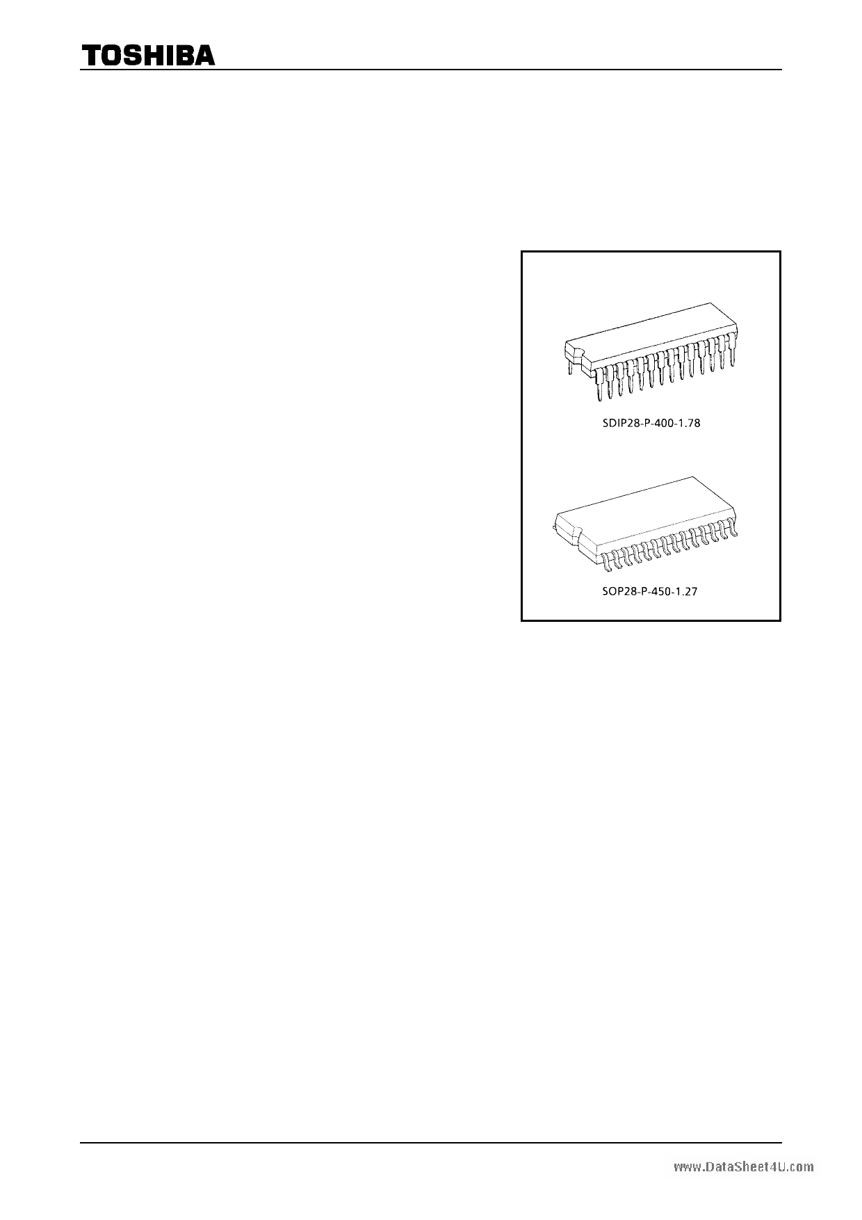
Weight
SDIP28-P-400-1.78 : 1.7 g (typ.)
SOP28-P-450-1.27 : 0.8 g (typ.)
• PLL detector for switching frequencies (fsc, 2 fsc, 4 fsc and 8 fsc clock inputs)
• 8-bit 4 fsc AD converter (2 channels)
• 10-bit 8 fsc DA converter (2 channels)
• 1-H delay line (2 channels)
• I2C bus control
• I2C bus decode output pin (High/Low)
• 5-V single power operation
1 2002-12-04
1 page 
www.DataSheet4U.com
Pin
No.
Pin Name
Function
DC Level
(V)
TC90A80N/F
Interface Circuit
MODE1 output pin
18 MODE1 High or Low output voltage signal can be selected
using I2C bus. Use for controlling peripheral circuits.
―
18
Clock input pin
19
FSC
Apply sine wave locked to the frequency of the input
video burst signal. One
2fsc, 4fsc, and 8fsc) can
obfethseelfeocutredfreuqsuinegncI2iCesb(ufssc.,
2.45
20
VDD5
PLL power supply pin (analog)
21
VSS5
PLL GND pin (analog)
5.0
0.0
19 170 Ω
300 kΩ
―
―
VCO control pin
22 FIL Connect lag-lead filter between this pin and pin 21
(VSS5).
3.0
90 Ω
22
100 Ω
DAC power supply pin (analog)
23
VDD2
Apply the same voltage as that of pin 3 (VDD1).
5.0 Internally connected to pin 3 (VDD1).
DAC bias 2 pin
24 VB2 Connect a 0.01-µF capacitor between this pin and pin
26 (VSS2).
3.4
24
Luminance signal output pin
25
YOUT
When Y/C Re-Mix Mode is selected using I2C bus, this
pin drives out a composite video signal.
Sync Tip
: 2.46
25
DAC GND pin (analog)
26
VSS2
Set the same voltage as that of pin 5 (VSS1).
0.0 Internally connected to pin 5 (VSS1).
5 2002-12-04
5 Page 
www.DataSheet4U.com
TC90A80N/F
Maximum Rating (Ta = 25°C)
Characteristics
Symbol
Rating
Unit
Supply voltage
Input voltage
Potential difference between power
supply pins
(Note 2)
Power dissipation
(Note 3)
TC90A80N
TC90A80F
Storage temperature
VDD
VIN
VDG
PD
Tstg
VSS + 6.0
VSS í 0.3 to VDD + 0.3
0.4
900
600
-55 to +125
V
V
V
mW
°C
Note 2: Connect pin 3 to pin 23. The potential difference among all power supply pins, 3 (23), 12, 13, and 20, must
not exceed 0.4 V.
The potential difference among VSS pins 5, 10, 21, and 26 must not exceed 0.01 V.
Note 3: Ta = 75°C for TC90A80F mounted on a PCB (70 mm × 70 mm × 1.6 mm)
Recommended Operating Conditions
Characteristics
Symbol
Min Typ. Max Unit
Supply voltage
Potential difference between pins 3
and 23
(Note 4)
Potential difference among power
supply pins 3,12, 13, and 20
Potential difference among VSS pins
5, 10, 21, and 26
Input voltage
Operating temperature
VDD
VDG1
VDG2
VSG
VIN
Topr
4.75 5.00 5.25
ʊ 0 0.04
ʊ 0 0.15
ʊ 0 0.01
0 ʊ VDD
í10 ʊ
75
V
V
V
V
V
°C
Note 4: Since power supply pins 3 and 23 are connected in the IC, supply power to them at the same voltage.
If there is a large potential difference between the pins, a large current flows through the IC causing
degradation or damage due to heat stress.
Maximum ratings: A set of specified parameter values which must not be exceeded during operation, even for an
instant. If any of these limit values is exceeded during operation, it causes permanent damage to
the TC90A80N/F. Therefore, care must be exercised that the TC90A80N/F operates within the
specified ranges.
Recommended operating conditions: Minimum, typical and maximum values for key operating parameters such as
supply voltage, DC voltage and operating temperature. Ensuring that the
parameter values remain within these specified ranges during operation will
help to ensure that the integrity of the TC90A80N/F is not compromised. When
designing video equipment, be aware that the TC90A80N/F can function within
the recommended operating ranges.
11 2002-12-04
11 Page | ||
| Páginas | Total 23 Páginas | |
| PDF Descargar | [ Datasheet TC90A80F.PDF ] | |
Hoja de datos destacado
| Número de pieza | Descripción | Fabricantes |
| TC90A80F | 3-Line Digital Comb Filter | Toshiba Semiconductor |
| TC90A80N | 3-Line Digital Comb Filter | Toshiba Semiconductor |
| Número de pieza | Descripción | Fabricantes |
| SLA6805M | High Voltage 3 phase Motor Driver IC. |
Sanken |
| SDC1742 | 12- and 14-Bit Hybrid Synchro / Resolver-to-Digital Converters. |
Analog Devices |
|
DataSheet.es es una pagina web que funciona como un repositorio de manuales o hoja de datos de muchos de los productos más populares, |
| DataSheet.es | 2020 | Privacy Policy | Contacto | Buscar |