|
|
PDF DEI1075 Data sheet ( Hoja de datos )
| Número de pieza | DEI1075 | |
| Descripción | (DEI1073 - DEI1075) Arinc 429 Line Driver | |
| Fabricantes | Device Engineering | |
| Logotipo |  |
|
Hay una vista previa y un enlace de descarga de DEI1075 (archivo pdf) en la parte inferior de esta página. Total 8 Páginas | ||
|
No Preview Available !
www.DataSheet4U.com
Device
Engineering
Incorporated
385 East Alamo Drive
Chandler, AZ 85225
Phone: (480) 303-0822
Fax: (480) 303-0824
E-mail: [email protected]
DEI1073, DEI1074, DEI1075
ARINC 429 LINE DRIVER WITH RATE
SELECT AND TRI-STATE
FEATURES
• TTL/CMOS TO ARINC 429 Line Driver.
• Rate control input set Hi (100KBS) or Lo (12.5KBS) speed slew rates.
• Operates from ±9.5V to ±16.5V power supply.
• Drives full ARINC load.
• Output resistor options: 0, 10 or 37.5 Ohms.
• Tristate Outputs
• Thermally enhanced 8 lead SOIC package.
• Outputs Short Circuit Tolerant
GENERAL DESCRIPTION
The DEI1073 family of 8 pin BiCMOS integrated circuits are line drivers designed to directly drive the ARINC 429 avionics
serial digital data bus. The device converts TTL/CMOS serial input data to the tri-level RZ bipolar differential modulation
format of the ARINC bus. The outputs are tri-state capable. A TTL/CMOS control input selects the output slew rate for HI
(100KBS) and LOW (12.5KBS) speed operation. No external timing capacitors are required.
The DEI1073 has internal 37.5 Ohm output resistors, the DEI1074 has 10 Ohm resistors, and the DEI1075 has none. The 10
and 0 Ohm options require external series resistors which are typically used to implement a transient voltage protection
network.
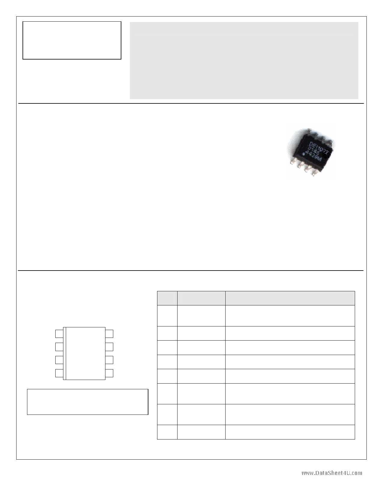
HI/LO 1
TTLIN0 2
TTLIN1 3
GND 4
8 V+
7 429OUTB
6 429OUTA
5 V-
Note:
Heatsink pad is electrically Isolated.
Table 1 PIN DESCRIPTION
PIN NAME
DESCRIPTION
1
HI/LO
LOGIC INPUT. Slew rate control. 1 = Hi speed. 0
= Low speed.
2
TTLIN0
LOGIC INPUT. Serial digital data input 0.
3
TTLIN1
LOGIC INPUT. Serial digital data input 1.
4
GND
POWER INPUT. Ground.
5 V- POWER INPUT. –9.5 to –16.5 VDC
6
429OUTA
429 OUTPUT. ARINC 429 format serial digital data
output A.
7
429OUTB
429 OUTPUT. ARINC 429 format serial digital data
output B.
8 V+ POWER INPUT. +9.5 to +16.5 VDC.
©2004 Device Engineering Inc
Page 1 of 8
DS-MW-01073-01 Rev C
05/31/2005
1 page 
www.DataSheet4U.com
DESIGN CONSIDERATIONS
Transient Voltage Protection
External transient voltage suppressing devices are required to protect the device from stress such as that defined by DO160D
Section 22, Lightning Induced Transient Susceptibility. The output stage of the driver includes intrinsic clamp diodes to the
V+ and V- power rails. Consider using the 0 Ohm output option to allow use of an external 36 Ohm current limiting resistor
and transient voltage suppressor. Transients at the device must be limited to less than one diode drop beyond the power rails to
prevent excessive current to the device.
Thermal Management
Device power dissipation varies greatly as a function of data rate, load capacitance, data duty cycle, and supply voltage. Proper
thermal management is important in designs operating at the HI speed data rate (100KBS) with high capacitive loads and high
data duty cycles. Dissipation may be estimated from the graph below which shows the approximate power dissipation for
various loads and supply voltages. It is calculated for 100% data duty cycle at 100KBS with no word gap null times and must
be reduced by the appropriate data duty cycle. Adjust for the application data duty cycle using a factor of (total bits transmitted
in 10 sec period / 1,000,000) = (32 x total ARINC words transmitted in 10 sec period / 1,000,000).
Heat transfer from the IC package should be maximized. Use maximum trace width on all power and signal connections at the
IC. The exposed heat sink pad of the SOIC package should be soldered to a heat spreader land on the PCB. The pad is
electrically isolated. Maximize land size by extending beyond the IC outline if possible. Place vias on the signal/power traces
close to the IC and on the heat spreader land to maximize heat flow to the internal power planes.
429 DRIVER DEVICE POWER DISSIPATION (100kbs, 100% DC)
1.6
1.4
1.2
1
100KHz, Full Load (30nF/400Ohm)
0.8 100KHz, 2/3 Load (20nF/600Ohm)
100KHz, 1/3 Load (10nF/1200Ohm)
0.6
0.4
0.2
0
7 8 9 10 11 12 13 14 15 16
Supply Voltage (+ / - V)
©2004 Device Engineering Inc
Page 5 of 8
DS-MW-01073-01 Rev C
05/31/2005
5 Page | ||
| Páginas | Total 8 Páginas | |
| PDF Descargar | [ Datasheet DEI1075.PDF ] | |
Hoja de datos destacado
| Número de pieza | Descripción | Fabricantes |
| DEI1073 | (DEI1073 - DEI1075) Arinc 429 Line Driver | Device Engineering |
| DEI1074 | (DEI1073 - DEI1075) Arinc 429 Line Driver | Device Engineering |
| DEI1075 | (DEI1073 - DEI1075) Arinc 429 Line Driver | Device Engineering |
| Número de pieza | Descripción | Fabricantes |
| SLA6805M | High Voltage 3 phase Motor Driver IC. |
Sanken |
| SDC1742 | 12- and 14-Bit Hybrid Synchro / Resolver-to-Digital Converters. |
Analog Devices |
|
DataSheet.es es una pagina web que funciona como un repositorio de manuales o hoja de datos de muchos de los productos más populares, |
| DataSheet.es | 2020 | Privacy Policy | Contacto | Buscar |
