|
|
|
PDF DFA100N75 Data sheet ( Hoja de datos )
| Número de pieza | DFA100N75 | |
| Descripción | N-Channel MOSFET | |
| Fabricantes | DnI | |
| Logotipo | ||
Hay una vista previa y un enlace de descarga de DFA100N75 (archivo pdf) en la parte inferior de esta página. Total 7 Páginas | ||
|
No Preview Available !
www.DataSheet4U.com
PRILIMINARY
DFA100N75
N-Channel MOSFET
Features
■ Low RDS(on) (0.013Ω )@VGS=10V
■ Low Gate Charge (Typical 90nC)
■ Low Crss (Typical 215pF)
■ Improved dv/dt Capability
■ 100% Avalanche Tested
■ Maximum Junction Temperature Range
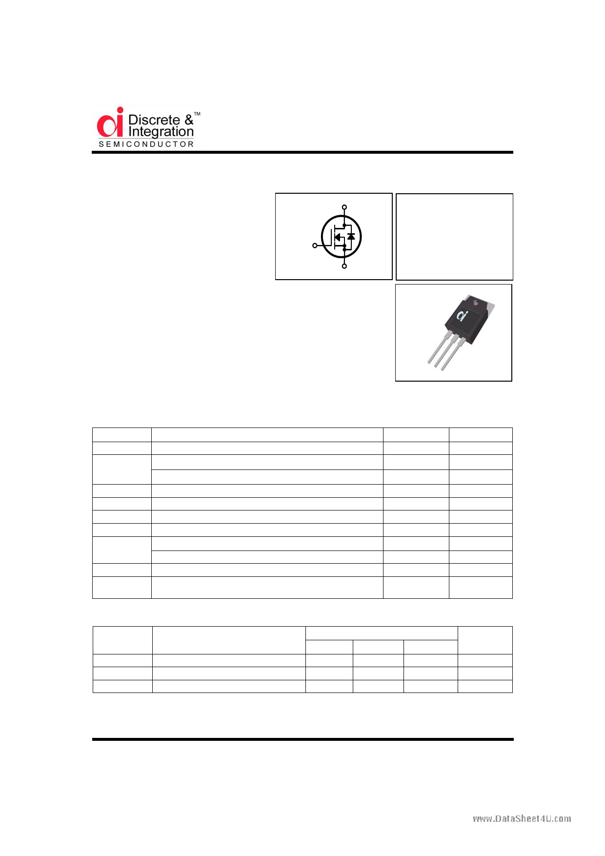
1.Gate
2.Drain
3.Source
General Description
This N-channel enhancement mode field-effect power transistor using D&I
semiconductor’s advanced planar stripe, DMOS technology intended for
battery operated systems like a DC-DC converter motor control, ups, etc.,
Also, especially designed to minimize rds(on) , low gate charge and high
rugged avalanche characteristics.
BVDSS =75V
RDS(ON) = 0.013 ohm
ID = 97A
TO-3P
123
Absolute Maximum Ratings
Symbol
VDSS
ID
IDM
VGS
EAS
dv/dt
PD
TSTG, TJ
TL
Parameter
Drain to Source Voltage
Continuous Drain Current(@TC = 25°C)
Continuous Drain Current(@TC = 100°C)
Drain Current Pulsed
Gate to Source Voltage
Single Pulsed Avalanche Energy
Peak Diode Recovery dv/dt
Total Power Dissipation(@TC = 25 °C)
Derating Factor above 25 °C
Operating Junction Temperature & Storage Temperature
Maximum Lead Temperature for soldering purpose,
1/8 from Case for 5 seconds.
Thermal Characteristics
Symbol
RθJC
RθCS
RθJA
Parameter
Thermal Resistance, Junction-to-Case
Thermal Resistance, Case to Sink
Thermal Resistance, Junction-to-Ambient
Min.
-
0.24
-
(Note 1)
(Note 2)
(Note 3)
Value
75
97
69
388
±20
2110
7.0
246
1.64
- 55 ~ 175
300
Value
Typ.
-
-
-
Max.
0.61
-
40
Units
V
A
A
A
V
mJ
V/ns
W
W/°C
°C
°C
Units
°C/W
°C/W
°C/W
March, 2006. Rev.0.
Copyright@ D&I Semiconductor Co., Ltd., All rights reserved.
1/7
1 page 
www.DataSheet4U.com
DFA100N75
Fig. 12. Gate Charge Test Circuit & Waveforms
12V 200nF 50KO
Same Type
as DUT
VGS
300nF
VGS
VDS
Qgs
DUT
1mA
Qg
Qgd
Charge
Fig 13. Switching Time Test Circuit & Waveforms
VDS
10V
Pulse
RG
Generator
RL
VDD
(0.5 rated VDS)
DUT
VDS 90%
10%
Vin
td(on)
tr
ton
td(off)
tf
toff
Fig 14. Unclamped Inductive Switching Test Circuit & Waveforms
10V
VDS
ID
RG
L
DUT
VDD
1 BVDSS
EAS = LL IAS2
2 BVDSS - VDD
BVDSS
IAS
ID(t)
tp
VDS(t)
Time
5/7
5 Page | ||
| Páginas | Total 7 Páginas | |
| PDF Descargar | [ Datasheet DFA100N75.PDF ] | |
Hoja de datos destacado
| Número de pieza | Descripción | Fabricantes |
| DFA100N75 | N-Channel MOSFET | DnI |
| Número de pieza | Descripción | Fabricantes |
| SLA6805M | High Voltage 3 phase Motor Driver IC. |
Sanken |
| SDC1742 | 12- and 14-Bit Hybrid Synchro / Resolver-to-Digital Converters. |
Analog Devices |
|
DataSheet.es es una pagina web que funciona como un repositorio de manuales o hoja de datos de muchos de los productos más populares, |
| DataSheet.es | 2020 | Privacy Policy | Contacto | Buscar |