|
|
|
PDF DS10CP154 Data sheet ( Hoja de datos )
| Número de pieza | DS10CP154 | |
| Descripción | 1.5 Gbps LVDS Crosspoint Switch | |
| Fabricantes | National Semiconductor | |
| Logotipo | ||
Hay una vista previa y un enlace de descarga de DS10CP154 (archivo pdf) en la parte inferior de esta página. Total 18 Páginas | ||
|
No Preview Available !
www.DataSheet4U.com
August 2007
DS10CP154
1.5 Gbps LVDS Crosspoint Switch
General Description
The DS10CP154 is a 1.5 Gbps 4x4 LVDS crosspoint switch
optimized for high-speed signal routing and switching over
FR-4 printed circuit board backplanes and balanced cables.
Fully differential signal paths ensure exceptional signal in-
tegrity and noise immunity. The non-blocking architecture
allows connections of any input to any output or outputs. The
switch configuration can be accomplished via external pins or
the System Management Bus (SMBus) interface. In addition,
the SMBus circuitry enables the loss of signal (LOS) monitors
that can inform a system of the presence of an open inputs
condition (e.g. disconnected cable).
Wide input common mode range allows the switch to accept
signals with LVDS, CML and LVPECL levels; the output levels
are LVDS. A very small package footprint requires a minimal
space on the board while the flow-through pinout allows easy
board layout. Each differential input and output is internally
terminated with a 100Ω resistor to lower device insertion and
return losses, reduce component count and further minimize
board space.
Features
■ DC - 1.5 Gbps low jitter, low skew, low power operation
■ Pin and SMBus configurable, fully differential, non-
blocking architecture
■ Wide input common mode range enables DC coupled
interface to CML or LVPECL drivers
■ LOS circuitry detects open inputs fault condition
■ On-chip 100 Ω input and output termination minimizes
insertion and return losses, reduces component count and
minimizes board space
■ 8 kV ESD on LVDS I/O pins protects adjoining
components
■ Small 6 mm x 6 mm 40-LLP space saving package
Applications
■ High-speed channel select applications
■ Clock and data buffering and muxing
■ SD / HD SDI Routers
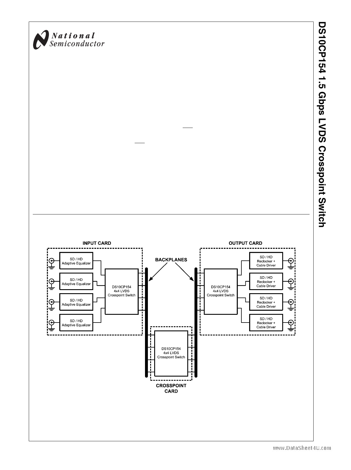
Typical Application
© 2007 National Semiconductor Corporation 300066
30006603
www.national.com
1 page 
www.DataSheet4U.com
Symbol
Parameter
LVDS OUTPUT DC SPECIFICATIONS
VOD
ΔVOD
Differential Output Voltage
Change in Magnitude of VOD for Complimentary
Output States
VOS
ΔVOS
Offset Voltage
Change in Magnitude of VOS for Complimentary
Output States
IOS Output Short Circuit Current (Note 8)
COUT Output Capacitance
ROUT Output Termination Resistor
SUPPLY CURRENT
ICC1 Supply Current
ICC2 Supply Current
ICC3 Supply Current
Conditions
RL = 100Ω
RL = 100Ω
OUT to GND
OUT to VCC
Any LVDS Output Pin to GND
Between OUT+ and OUT-
PWDN = 0
PWDN = 1
Broadcast Mode (1:4)
PWDN = 1
Quad Buffer Mode (4:4)
Min Typ Max Units
250
-35
1.05
-35
350 450
35
1.2 1.375
35
-25 -55
7 55
1.2
100
mV
mV
V
mV
mA
mA
pF
Ω
40 50
103 125
mA
mA
115 140 mA
Note 4: “Absolute Maximum Ratings” indicate limits beyond which damage to the device may occur, including inoperability and degradation of device reliability
and/or performance. Functional operation of the device and/or non-degradation at the Absolute Maximum Ratings or other conditions beyond those indicated in
the Recommended Operating Conditions is not implied. The Recommended Operating Conditions indicate conditions at which the device is functional and the
device should not be operated beyond such conditions.
Note 5: The Electrical Characteristics tables list guaranteed specifications under the listed Recommended Operating Conditions except as otherwise modified
or specified by the Electrical Characteristics Conditions and/or Notes. Typical specifications are estimations only and are not guaranteed.
Note 6: Current into device pins is defined as positive. Current out of device pins is defined as negative. All voltages are referenced to ground except VOD and
ΔVOD.
Note 7: Typical values represent most likely parametric norms for VCC = +3.3V and TA = +25°C, and at the Recommended Operation Conditions at the time of
product characterization and are not guaranteed.
Note 8: Output short circuit current (IOS) is specified as magnitude only, minus sign indicates direction only.
5 www.national.com
5 Page 
www.DataSheet4U.com
REGISTER DESCRIPTIONS
There are three data registers in the DS10CP154 accessible via the SMBus interface.
Address
(hex)
0
3
4
Name
Switch Configuration
Control
LOS
TABLE 6. DS10CP154 SMBus Data Registers
Access Description
R/W
R/W
RO
Switch Configuration Register
Powerdown, LOS Enable and Pin Control Register
Loss Of Signal (LOS) Reporting Register
30006610
FIGURE 5. DS10CP154 Registers Block Diagram
11 www.national.com
11 Page | ||
| Páginas | Total 18 Páginas | |
| PDF Descargar | [ Datasheet DS10CP154.PDF ] | |
Hoja de datos destacado
| Número de pieza | Descripción | Fabricantes |
| DS10CP152 | DS10CP152 1.5 Gbps 2X2 LVDS Crosspoint Switch (Rev. E) | Texas Instruments |
| DS10CP152 | 1.5 Gbps 2X2 LVDS Crosspoint Switch | National Semiconductor |
| DS10CP152Q | DS10CP152Q Automotive 1.5 Gbps 2X2 LVDS Crosspoint Switch (Rev. E) | Texas Instruments |
| DS10CP152Q | Automotive 1.5 Gbps 2X2 LVDS Crosspoint Switch | National Semiconductor |
| Número de pieza | Descripción | Fabricantes |
| SLA6805M | High Voltage 3 phase Motor Driver IC. |
Sanken |
| SDC1742 | 12- and 14-Bit Hybrid Synchro / Resolver-to-Digital Converters. |
Analog Devices |
|
DataSheet.es es una pagina web que funciona como un repositorio de manuales o hoja de datos de muchos de los productos más populares, |
| DataSheet.es | 2020 | Privacy Policy | Contacto | Buscar |