|
|
PDF TDA9965A Data sheet ( Hoja de datos )
| Número de pieza | TDA9965A | |
| Descripción | 40 Msps analog-to-digital interface for CCD cameras | |
| Fabricantes | NXP Semiconductors | |
| Logotipo | ||
Hay una vista previa y un enlace de descarga de TDA9965A (archivo pdf) en la parte inferior de esta página. Total 22 Páginas | ||
|
No Preview Available !
www.DataSheet4U.com
INTEGRATED CIRCUITS
DATA SHEET
TDA9965A
12-bit, 5.0 V, 40 Msps
analog-to-digital interface for CCD
cameras
Product specification
Supersedes data of 2003 Nov 26
2004 Jul 05
1 page 
www.DataSheet4U.com
Philips Semiconductors
12-bit, 5.0 V, 40 Msps analog-to-digital
interface for CCD cameras
SYMBOL
VCCD1
DGND1
CLKADC
CLPADC
CLPOB
SHP
SHD
VCCD2
DGND2
PIN DESCRIPTION
40 digital supply voltage 1
41 digital ground 1
42 ADC clock input
43 clamp control pulse input for ADC analog input signal
44 clamp control pulse input at optical black
45 preset sample and hold pulse input
46 data sample and hold pulse input
47 digital supply voltage 2
48 digital ground 2
Product specification
TDA9965A
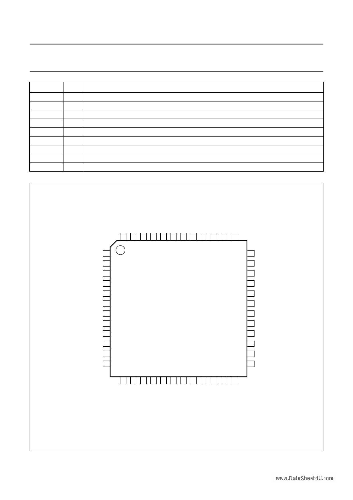
handbook, full pagewidth
AGND4 1
IN 2
AGND5 3
STGE 4
AGND1 5
VCCA1 6
AGND2 7
VCCA2 8
Vref 9
PGAOUT 10
ADCIN 11
n.c. 12
TDA9965AHL
36 D9
35 D8
34 D7
33 D6
32 VCCO2
31 OGND2
30 VCCO1
29 OGND1
28 D5
27 D4
26 D3
25 D2
MGU715
2004 Jul 05
Fig.2 Pin configuration.
5
5 Page 
www.DataSheet4U.com
Philips Semiconductors
12-bit, 5.0 V, 40 Msps analog-to-digital
interface for CCD cameras
Product specification
TDA9965A
Table 1 Serial interface programming
ADDRESS BITS
A1 A0
00
01
10
11
SDATA BITS SD0 to SD9
clamp reference of ADC (SD0 to SD9); note 1
cut-off frequency of CTH (SD0 to SD3)
PGA gain control (SD0 to SD9)
edge control for pulses SHP, SHD, CLPOB, CLPADC and CLKADC (note 2):
SD0 = 1, SHP and SHD sample on LOW level
SD1 = 1, CLPADC and CLPOB activated on HIGH level
SD2 = 1, CLKADC activated with rising edge
Notes
1. PGA gain register must always be refreshed after clamp code register content has been changed.
2. When pin CLPADC = HIGH (SD1 = 1; serial interface), the ADC input is clamped to the voltage level of Vref. Pin Vref
is connected to ground via a capacitor.
When the power supplies increase from zero to VCC, the init-on-power block initializes the circuit as follows:
• Cut-off frequency of the CTH circuit is set to: code fco(CTH) = 0
• PGA gain control is set to: code GPGA = 0
• Clamp code of the ADC is set to: code ADCCLP = 0
• SHP and SHD sample on HIGH level; CLKADC activated with rising edge
• CLPOB and CLPADC activated on HIGH level.
Table 2 Standby selection
PIN STDBY
HIGH
LOW
DATA BITS SD9 to SD0
logic 0
active
ICCA + ICCD
4 mA (typical); note 1
84 mA (typical)
Note
1. If an external regulator is used it has to be switched off in standby mode in order to avoid extra power consumption
by the TDA9965A.
2004 Jul 05
11
11 Page | ||
| Páginas | Total 22 Páginas | |
| PDF Descargar | [ Datasheet TDA9965A.PDF ] | |
Hoja de datos destacado
| Número de pieza | Descripción | Fabricantes |
| TDA9965 | 30 Msps analog-to-digital interface for CCD cameras | NXP Semiconductors |
| TDA9965A | 40 Msps analog-to-digital interface for CCD cameras | NXP Semiconductors |
| Número de pieza | Descripción | Fabricantes |
| SLA6805M | High Voltage 3 phase Motor Driver IC. |
Sanken |
| SDC1742 | 12- and 14-Bit Hybrid Synchro / Resolver-to-Digital Converters. |
Analog Devices |
|
DataSheet.es es una pagina web que funciona como un repositorio de manuales o hoja de datos de muchos de los productos más populares, |
| DataSheet.es | 2020 | Privacy Policy | Contacto | Buscar |
