|
|
|
PDF TB6581H Data sheet ( Hoja de datos )
| Número de pieza | TB6581H | |
| Descripción | 3-Phase Full-Wave Sine-Wave PWM Brushless Motor Controller | |
| Fabricantes | Toshiba Semiconductor | |
| Logotipo | ||
Hay una vista previa y un enlace de descarga de TB6581H (archivo pdf) en la parte inferior de esta página. Total 14 Páginas | ||
|
No Preview Available !
www.DataSheet4U.com
TB6581H/HG
TOSHIBA Bi-CMOS Power Integrated Circuit Multi-Chip Package (MCP)
TB6581H/HG
3-Phase Full-Wave Sine-Wave PWM Brushless Motor Controller
The TB6581H/HG is a high-voltage PWM BLDC motor driver.
The product integrates the TB6551F/FG sine-wave controller and
the TPD4103AK high-voltage driver in a single package (“2-in-1”).
It is designed to change the speed of a BLDC directly motor by
using a speed control signal (analog) from a microcontroller.
Features
• A sine wave PWM drive controller and a high-voltage driver
integrated in a single package.
• IGBTs arranged in three half-bridge units
• Triangle wave generator (carrier frequency = fosc/254 (Hz))
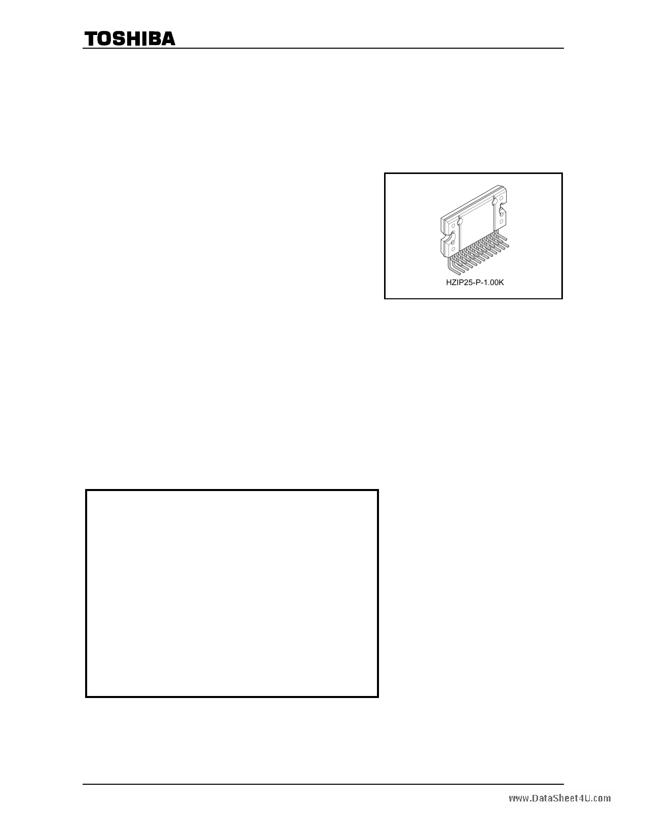
Weight:
• Dead-time insertion (1.9 µs)
HZIP25-P-1.00K: 7.7 g (typ.)
• High-side bootstrap supply
• Bootstrap diode
• Overcurrent protection, thermal shutdown, and undervoltage lockout
• On-chip regulator (Vreg = 7 V (typ.), 30 mA (max),
Vrefout = 5 V (typ.), 30 mA (max))
• Operating power supply voltage range: VCC = 13.5~16.5 V
• Motor power supply operating voltage range: VB = 50~400 V
TB6581HG:
TB6581HG is a Pb-free product.
The following conditions apply to solderability:
*Solderability
1. Use of Sn-63Pb solder bath
*solder bath temperature = 230˚C
*dipping time = 5 seconds
*number of times = once
*use of R-type flux
2. Use of Sn-3.0Ag-0.5Cu solder bath
*solder bath temperature = 245˚C
*dipping time = 5 seconds
*the number of times = once
*use of R-type flux
1 2004-03-01
1 page 
www.DataSheet4U.com
TB6581H/HG
Electrical Characteristics (Ta = 25°C)
Characteristics
Symbol
Test Condition
Min Typ. Max Unit
Current dissipation
Input current
Input voltage
IB
ICC15
ICC7
IBS (ON)
IBS (OFF)
Iin (LA)
Iin (Ve)
Iin (Hall)
VB = 400 V
Vreg = OPEN, VCC = 15 V
Vrefout = OPEN, VCC = 7 V
VBS = 15 V, high-side ON
VBS = 15 V, high-side OFF
Vin = 5 V, LA
Vin = 5 V, Ve
Vin = 0 V, HU, HV, HW
Vin
(Hall)
HIGH
HU, HV, HW
LOW
HIGH PWM Duty 100%
Vin
(Ve)
Middle Refresh → Start motor operation
LOW Turned-off → Refresh
⎯ 0.1 0.5
⎯ 1.1
3
⎯3
6
⎯ 260 410
⎯ 230 370
⎯ 25 50
⎯ 35 70
−50 −25 ⎯
Vrefout
−1
⎯
Vrefout
⎯ ⎯ 0.8
5.1 5.4 5.7
1.8 2.1 2.4
0.7 1.0 1.3
Input hysteresis voltage
Input delay time
Output saturation voltage
VH
VDT
VDC
VCEsatH
VCEsatL
VFG (H)
HU, HV, HW
(Note 6) ⎯
0.3
HU, HV, HW
Xin = 4.19 MHz
⎯ 4.0
Idc
Xin = 4.19 MHz
⎯ 4.0
VCC = 15 V, IC = 0.5 A
⎯ 2.4
VCC = 15 V, IC = 0.5 A
⎯ 2.4
IOUT = 1 mA
FG
Vrefout Vrefout
− 1.0 − 0.2
⎯
⎯
⎯
3
3
⎯
Output voltage
FRD forward voltage
BSD forward voltage
Current detection
Thermal shutdown protection
VFG (L) IOUT = −1 mA
FG
⎯ 0.2 1.0
Vrefout
IOUT = 30 mA
Vrefout
4.5 5.0 5.5
Vreg
IOUT = 30 mA
6.5 7 7.5
VFH IF = 0.5 A, high-side
⎯ 1.3 2.0
VFL IF = 0.5 A, low-side
⎯ 1.3 2.0
VF (BSD) IF = 500 µA
⎯ 0.9 1.2
Vdc Idc
0.47 0.5 0.53
TSD
TSDhys
150 165 200
(Note 7)
⎯ 20 ⎯
VCC15 undervoltage protection for
driver
VBS undervoltage protection for driver
VCC15 (H)
VCC15 (L)
VBS (H)
VBS (L)
Undervoltage positive-going threshold
Undervoltage negative-going threshold
Undervoltage positive-going threshold
Undervoltage negative-going threshold
10.5
10
8.5
8
11.5
11
9.5
9
12.5
12
10.5
10
VCC7 undervoltage protection for
controller
Output turn-on/-off delay time
Dead time
FRD reverse recovery time
VCC7 (H) Undervoltage positive-going threshold 4.2 4.5 4.8
VCC7 (L) Undervoltage negative-going threshold 3.7 4.0 4.3
ton
VBB = 280 V, VCC = 15 V, IC = 0.5 A
⎯ 1.5
3
toff VBB = 280 V, VCC = 15 V, IC = 0.5 A ⎯ 1.2 3
tdead
Xin = 4.19 MHz
1.5 1.8 ⎯
trr
VBB = 280 V, VCC = 15 V, IC = 0.5 A
⎯ 200 ⎯
mA
µA
µA
V
V
µs
V
V
V
V
V
°C
V
V
V
µs
µs
ns
Note 6 and Note 7: Toshiba does not implement testing before shipping.
5 2004-03-01
5 Page 
www.DataSheet4U.com
TB6581H/HG
External Parts
Symbol
Purpose
Recommended value
Note
X1
C1, C2, C3
R1, R2, R3
C4
C5
R4
R5
C6
C7
C8
C9
C10, C11, C12
Internal clock generation
Noise absorber
Vrefout oscillation protection
Noise absorber
Overcurrent detection
VREG power supply stability
VCC15 power supply stability
Bootstrap capacitor
4.19 MHz
10 V/1000 pF
10 kΩ
10 V/0.1 µF~1.0 µF
10 V/1000pF
5.1 kΩ
0.62 Ω ± 1% (1 W)
16 V/1.0 µF~10 µF
10 V/1000 pF
25 V/0.1 µF
25 V/10 µF
25 V/2.2 µF
(Note 1)
(Note 2)
(Note 3)
(Note 2)
(Note 4)
(Note 3)
(Note 3)
(Note 5)
Note 1: For carrier frequency and dead time, connect a 4.19 MHz ceramic resonator.
Note 2: These parts are used as a low-pass filter for noise absorption. Test to confirm noise filtering, then set the
filter time-constant.
Note 3: This part is used as a capacitor for power supply stability. Adjust the part to the application environment as
required. When mounting, place it as close as possible to the base of the leads of this product to improve
the noise elimination.
Note 4: This part is used to set the value for overcurrent detection. Iout (max) = Vdc ÷ R5 (Vdc = 0.5 V (typ.))
Note 5: The required bootstrap capacitance value varies according to the motor drive conditions. The voltage stress
for the capacitor is the value of VCC15.
Other Precautions
A short circuit between the outputs, or between output and supply or ground may damage the device. Peripheral
parts may also be damaged by overvoltage and overcurrent. Design the output lines, VCC and GND lines so that
short circuits do not occur.
Also be careful not to insert the IC in the wrong direction because this could destroy the IC.
In turning on the power, first supply Vcc15 and confirm its stability; then apply Vcc7 and the driving input signal.
Vcc15 and VB may be turned on in either order. In turning off the power, take care not to cut off the VB line by
relay while the motor is spinning. Doing so may cause the IC to break down by cutting the current-producing route
for VB.
The TB6581H/HG is sensitive to electrostatic discharge. Handle with care.
The product should be mounted by the solder-flow method. The preheating time is from 60 to 120 seconds at
150˚C. The maximum heat is 260˚C, to be applied within 10 seconds and as far as the lead stopper.
11 03/12/25
11 Page | ||
| Páginas | Total 14 Páginas | |
| PDF Descargar | [ Datasheet TB6581H.PDF ] | |
Hoja de datos destacado
| Número de pieza | Descripción | Fabricantes |
| TB6581H | 3-Phase Full-Wave Sine-Wave PWM Brushless Motor Controller | Toshiba Semiconductor |
| TB6581HG | 3-Phase Full-Wave Sine-Wave PWM Brushless Motor Controller | Toshiba Semiconductor |
| Número de pieza | Descripción | Fabricantes |
| SLA6805M | High Voltage 3 phase Motor Driver IC. |
Sanken |
| SDC1742 | 12- and 14-Bit Hybrid Synchro / Resolver-to-Digital Converters. |
Analog Devices |
|
DataSheet.es es una pagina web que funciona como un repositorio de manuales o hoja de datos de muchos de los productos más populares, |
| DataSheet.es | 2020 | Privacy Policy | Contacto | Buscar |