|
|
|
PDF IDT70T3589S Data sheet ( Hoja de datos )
| Número de pieza | IDT70T3589S | |
| Descripción | (IDT70T3519 - IDT70T3599) HIGH-SPEED 2.5V 256/128/64K x 36 SYNCHRONOUS DUAL-PORT STATIC RAM | |
| Fabricantes | IDT | |
| Logotipo | ||
Hay una vista previa y un enlace de descarga de IDT70T3589S (archivo pdf) en la parte inferior de esta página. Total 28 Páginas | ||
|
No Preview Available !
www.DataSheet4U.com
HIGH-SPEED 2.5V
256/128/64K x 36
SYNCHRONOUS
IDT70T3519/99/89S
DUAL-PORT STATIC RAM
WITH 3.3V OR 2.5V INTERFACE
Features:
◆ True Dual-Port memory cells which allow simultaneous
access of the same memory location
◆ High-speed data access
– Commercial: 3.4 (200MHz)/3.6ns (166MHz)/
4.2ns (133MHz)(max.)
– Industrial: 3.6ns (166MHz)/4.2ns (133MHz) (max.)
◆ Selectable Pipelined or Flow-Through output mode
◆ Counter enable and repeat features
◆ Dual chip enables allow for depth expansion without
additional logic
◆ Interrupt and Collision Detection Flags
◆ Full synchronous operation on both ports
– 5ns cycle time, 200MHz operation (14Gbps bandwidth)
– Fast 3.4ns clock to data out
– 1.5ns setup to clock and 0.5ns hold on all control, data, and
address inputs @ 200MHz
– Data input, address, byte enable and control registers
– Self-timed write allows fast cycle time
◆ Separate byte controls for multiplexed bus and bus
matching compatibility
◆ Dual Cycle Deselect (DCD) for Pipelined Output Mode
◆ 2.5V (±100mV) power supply for core
◆ LVTTL compatible, selectable 3.3V (±150mV) or 2.5V
(±100mV) power supply for I/Os and control signals on
each port
◆ Industrial temperature range (-40°C to +85°C) is
available at 166MHz and 133MHz
◆ Available in a 256-pin Ball Grid Array (BGA), a 208-pin
Plastic Quad Flatpack (PQFP) and 208-pin fine pitch Ball
Grid Array (fpBGA)
◆ Supports JTAG features compliant with IEEE 1149.1
◆ Due to limited pin count JTAG is not supported on the 208-
pin PQFP package
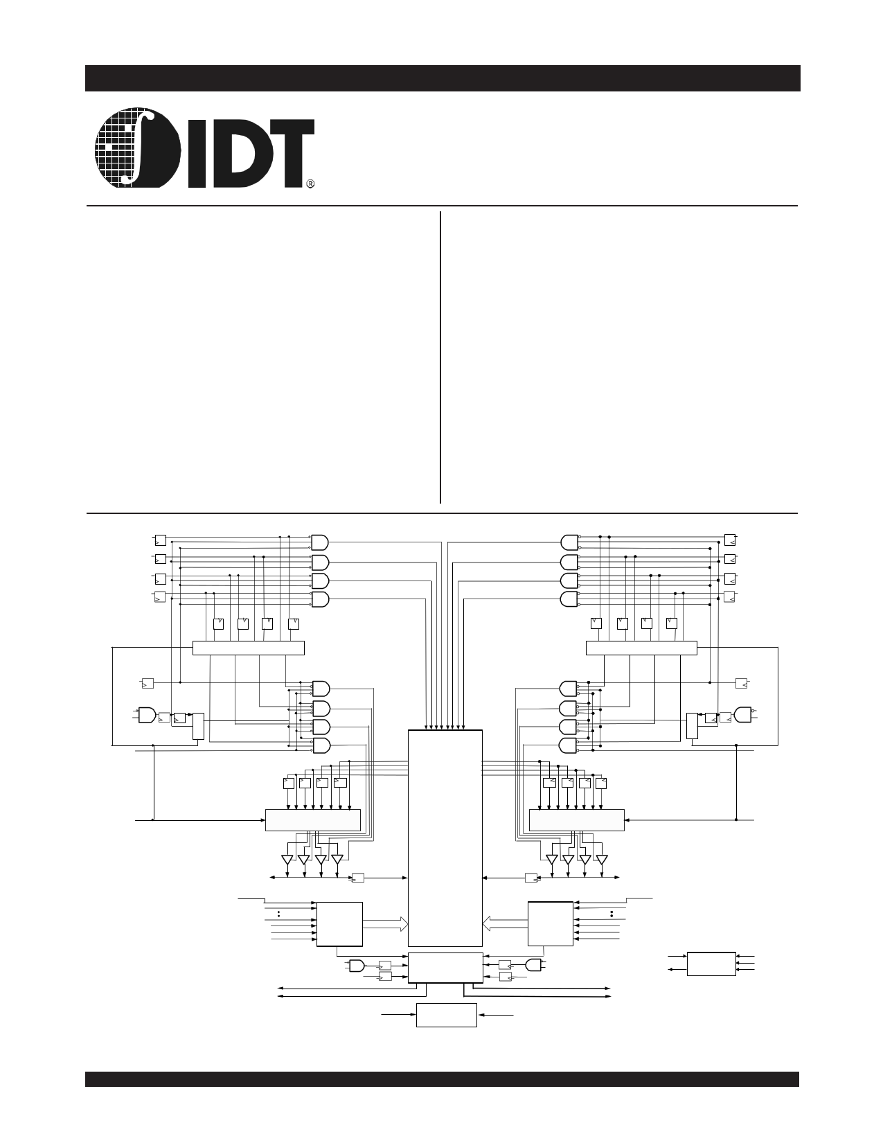
Functional Block Diagram
BE3L
BE3R
BE2L
BE2R
B E1 L
BE1R
BE0L
BE0R
FT/PIP EL
0a 1a
1/0
a
0b 1b 0c 1c
bc
0d 1d
d
1d 0d
d
1c 0c
c
1b 0b
b
1a 0a
1/0
a
FT/PIPER
R/WL
R/WR
CE0L
CE1L
OEL
1
0
1/0
FT/PIPEL
1d 0d 1c 0c 1b 0b 1a 0a
0/1
a bc d
BB BBBB BB
WW WWWW WW
01 2332 10
L L L L RR RR
Do ut0 -8 _L
Do ut9 -1 7_ L
Do ut1 8-26 _L
Do ut2 7-35 _L
D o ut0 -8 _R
D ou t9-17 _R
D out18-26_R
D out27-35_R
256/128/64K x 36
MEM ORY
ARRAY
0a 1a 0b 1b 0c 1c 0d 1d
dc b a
0/1
C E0 R
1 CE1R
0
1/0
OER
FT/PIPER
,
I/O0L - I/O35L
Din_L
Din_R
I/O0R - I/O35R
CLKL
A17L(1)
A0L
REPEATL
ADSL
CN TENL
Counter/
Address
Reg.
ADDR_L
ADDR_R
Counter/
Address
Reg.
CLKR
A17R(1)
A0R
REPE ATR
AD SR
CNTENR
COL L
INTL
CE 0 L
CE1L
R /WL
INTERRUPT
COLLISION
DETECTION
LOGIC
CE0 R
C E1 R
R/WR
COLR
INTR
NOTES:
ZZL(2)
ZZ
CONTROL
LOGIC
ZZ R(2)
1. Address A17 is a NC for the IDT70T3599. Also, Addresses A17 and A16 are NC's for the IDT70T3589.
2. The sleep mode pin shuts off all dynamic inputs, except JTAG inputs, when asserted. All static inputs, i.e., PL/FTx and OPTx
and the sleep mode pins themselves (ZZx) are not affected during sleep mode.
1
©2004 Integrated Device Technology, Inc.
TDI
TDO
,
JTAG
TCK
TMS
TRST
5666 drw 01
APRIL 2004
DSC 5666/6
1 page 
IDT70T3519/99/89S
High-Speed 2.5V 256/128/64K x 36 Dual-Port Synchronous Static RAM
Industrial and Commercial Temperature Ranges
Pin Configuration (3,4,5,6,9) (con't.)
01/23/03
A1 A2
A3 A4 A5
A6 A7
A8 A9
A10 A11 A12
A13 A14 A15 A16 A17
I/O19L I/O18L VSS TDO COLL A16L(2) A12L A8L BE1L VDD CLKL CNTENL A4L A0L OPTL I/O17L VSS
B1 B2 B3 B4 B5 B6 B7 B8 B9 B10 B11 B12 B13 B14 B15 B16 B17
I/O20R VSS I/O18R TDI A17L(1) A13L A9L BE2L CE0L VSS ADSL A5L A1L NC VDDQR I/O16L I/O15R
C1 C2 C3 C4 C5 C6 C7 C8 C9 C10 C11 C12 C13 C14 C15 C16 C17
VDDQL I/O19R VDDQR PL/FTL INTL A14L A10L BE3L CE1L VSS R/WL A6L A2L VDD I/O16R I/O15L VSS
D1 D2 D3 D4 D5 D6 D7 D8 D9 D10 D11 D12 D13 D14 D15 D16 D17
I/O22L VSS I/O21L I/O20L A15L A11L A7L BE0L VDD OEL REPEATL A3L VDD I/O17R VDDQL I/O14L I/O14R
E1 E2 E3 E4
I/O23L I/O22R VDDQR I/O21R
E14 E15 E16 E17
I/O12L I/O13R VSS I/O13L
F1 F2 F3 F4
VDDQL I/O23R I/O24L VSS
F14 F15 F16 F17
VSS I/O12R I/O11L VDDQR
G1 G2 G3 G4
I/O26L VSS I/O25L I/O24R
H1 H2 H3 H4
VDD I/O26R VDDQR I/O25R
J1 J2 J3 J4
VDDQL VDD VSS ZZR
K1 K2 K3 K4
I/O28R VSS I/O27R VSS
70T3519/99/89BF
BF-208(7)
208-Pin fpBGA
Top View(8)
G14 G15 G16 G17
I/O9L VDDQL I/O10L I/O11R
H14 H15 H16
H17
VDD I/O9R VSS I/O10R
J14 J15 J16 J17
ZZL VDD VSS VDDQR
K14 K15 K16 K17
I/O7R VDDQL I/O8R VSS
L1 L2 L3 L4
I/O29R I/O28L VDDQR I/O27L
L14 L15 L16 L17
I/O6R I/O7L VSS I/O8L
M1 M2 M3 M4
VDDQL I/O29L I/O30R VSS
N1 N2 N3 N4
I/O31L VSS I/O31R I/O30L
M14 M15 M16 M17
VSS I/O6L I/O5R VDDQR
N14 N15 N16 N17
I/O3R VDDQL I/O4R I/O5L
P1 P2 P3 P4 P5 P6 P7 P8 P9 P10 P11 P12 P13 P14 P15 P16 P17
I/O32R I/O32L VDDQR I/O35R TRST A16R(2) A12R A8R BE1R VDD CLKR C NTENR A4R I/O2L I/O3L VSS I/O4L
R1 R2 R3 R4 R5 R6 R7 R8 R9 R10 R11 R12 R13 R14 R15 R16 R17
VSS I/O33L I/O34R TCK A17R(1) A13R A9R BE2R CE0R VSS ADSR A5R A1R NC VDDQL I/O1R VDDQR
T1 T2 T3 T4 T5 T6 T7 T8 T9 T10 T11 T12 T13 T14 T15 T16 T17
I/O33R I/O34L VDDQL TMS INTR A14R A10R BE3R CE1R VSS R/WR A6R A2R VSS I/O0R VSS I/O2R
U1 U2 U3 U4 U5 U6 U7 U8 U9 U10
VSS I/O35L PL/FTR COLR A15R A11R A7R BE0R VDD OER
U12 U13 U14 U15 U16 U17
A3R A0R VDD OPTR I/O0L I/O1L
5666 drw 02c
NOTES:
1. Pin is a NC for IDT70T3599 and IDT70T3589.
2. Pin is a NC for IDT70T3589.
3. All VDD pins must be connected to 2.5V power supply.
4. All VDDQ pins must be connected to appropriate power supply: 3.3V if OPT pin for that port is set to VDD (2.5V), and 2.5V if OPT pin for that port is
set to VSS (0V).
5. All VSS pins must be connected to ground supply.
6. Package body is approximately 15mm x 15mm x 1.4mm with 0.8mm ball pitch.
7. This package code is used to reference the package diagram.
8. This text does not indicate orientation of the actual part-marking.
9. Pins B14 and R14 will be VREFL and VREFR respectively for future HSTL device.
6.452
5 Page 
IDT70T3519/99/89S
High-Speed 2.5V 256/128/64K x 36 Dual-Port Synchronous Static RAM
AC Test Conditions (VDDQ - 3.3V/2.5V)
Input Pulse Levels (Address & Controls) GND to 3.0V/GND to 2.4V
Input Pulse Levels (I/Os)
GND to 3.0V/GND to 2.4V
Input Rise/Fall Times
2ns
Input Timing Reference Levels
1.5V/1.25V
Output Reference Levels
1.5V/1.25V
Output Load
Figure 1
5666 tbl 10
Industrial and Commercial Temperature Ranges
DATAOUT
50Ω 50Ω
10pF
(Tester)
Figure 1. AC Output Test load.
,
1.5V/1.25
5666 drw 03
∆ tCD
(Typical, ns)
∆ Capacitance (pF) from AC Test Load 5666 drw 04
6.1412
11 Page | ||
| Páginas | Total 28 Páginas | |
| PDF Descargar | [ Datasheet IDT70T3589S.PDF ] | |
Hoja de datos destacado
| Número de pieza | Descripción | Fabricantes |
| IDT70T3589S | (IDT70T3519 - IDT70T3599) HIGH-SPEED 2.5V 256/128/64K x 36 SYNCHRONOUS DUAL-PORT STATIC RAM | IDT |
| Número de pieza | Descripción | Fabricantes |
| SLA6805M | High Voltage 3 phase Motor Driver IC. |
Sanken |
| SDC1742 | 12- and 14-Bit Hybrid Synchro / Resolver-to-Digital Converters. |
Analog Devices |
|
DataSheet.es es una pagina web que funciona como un repositorio de manuales o hoja de datos de muchos de los productos más populares, |
| DataSheet.es | 2020 | Privacy Policy | Contacto | Buscar |