|
|
|
PDF IDT2305A Data sheet ( Hoja de datos )
| Número de pieza | IDT2305A | |
| Descripción | 3.3V ZERO DELAY CLOCK BUFFER | |
| Fabricantes | IDT | |
| Logotipo | ||
Hay una vista previa y un enlace de descarga de IDT2305A (archivo pdf) en la parte inferior de esta página. Total 7 Páginas | ||
|
No Preview Available !
www.DataSheet4U.com
IDT2305A
3.3V ZERO DELAY CLOCK BUFFER
COMMERCIAL AND INDUSTRIAL TEMPERATURE RANGES
3.3V ZERO DELAY CLOCK
BUFFER
IDT2305A
FEATURES:
• Phase-Lock Loop Clock Distribution
• 10MHz to 133MHz operating frequency
• Distributes one clock input to one bank of five outputs
• Zero Input-Output Delay
• Output Skew < 250ps
• Low jitter <200 ps cycle-to-cycle
• IDT2305A-1 for Standard Drive
• IDT2305A-1H for High Drive
• No external RC network required
• Operates at 3.3V VDD
• Power down mode
• Available in SOIC package
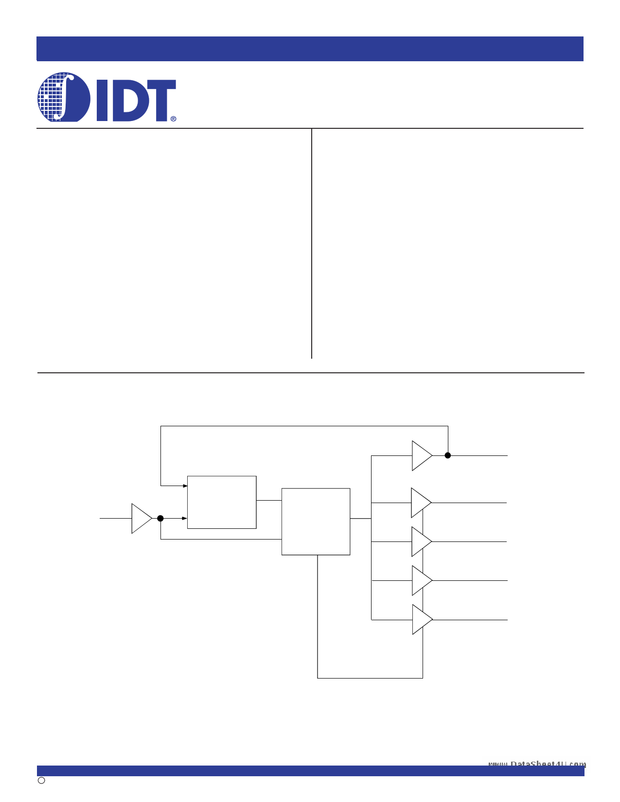
FUNCTIONAL BLOCK DIAGRAM
DESCRIPTION:
The IDT2305A is a high-speed phase-lock loop (PLL) clock buffer,
designed to address high-speed clock distribution applications. The zero
delay is achieved by aligning the phase between the incoming clock and
the output clock, operable within the range of 10 to 133MHz.
The IDT2305A is an 8-pin version of the IDT2309A. IDT2305A accepts
one reference input, and drives out five low skew clocks. The -1H version
of this device operates up to 133MHz frequency and has a higher drive than
the -1 device. All parts have on-chip PLLs which lock to an input clock on
the REF pin. The PLL feedback is on-chip and is obtained from the CLKOUT
pad. In the absence of an input clock, the IDT2305A enters power down.
In this mode, the device will draw less than 12µA for Commercial Tempera-
ture range and less than 25µA for Industrial temperature range, the outputs
are tri-stated, and the PLL is not running, resulting in a significant reduction
of power.
The IDT2305A is characterized for both Industrial and Commercial
operation.
REF 1
PLL
Control
Logic
8
CLKOUT
3 CLK1
2 CLK2
5 CLK3
7
CLK4
The IDT logo is a registered trademark of Integrated Device Technology, Inc.
COMMERCIAL AND INDUSTRIAL
c 2004 Integrated Device Technology, Inc.
TEMPERATURE
1
RANGES
JULY 2004
DSC 6586/3
1 page 
IDT2305A
3.3V ZERO DELAY CLOCK BUFFER
COMMERCIAL AND INDUSTRIAL TEMPERATURE RANGES
SWITCHING CHARACTERISTICS (2305A-1) - INDUSTRIAL(1,2)
Symbol
Parameter
Conditions
Min.
t1 Output Frequency
10pF Load
10
30pF Load
10
Duty Cycle = t2 ÷ t1
t3 Rise Time
Measured at 1.4V, FOUT = 66.66MHz
Measured between 0.8V and 2V
40
—
t4 Fall Time
Measured between 0.8V and 2V
—
t5 Output to Output Skew
All outputs equally loaded
—
t6 Delay, REF Rising Edge to CLKOUT Rising Edge Measured at VDD/2
—
t7 Device-to-Device Skew
Measured at VDD/2 on the CLKOUT pins of devices
—
tJ Cycle-to-Cycle Jitter, pk - pk
Measured at 66.66MHz, loaded outputs
—
tLOCK PLL Lock Time
Stable power supply, valid clock presented on REF pin —
Typ. Max.
— 133
— 100
50 60
— 2.5
— 2.5
— 250
0 ±350
0 700
— 200
—1
Unit
MHz
%
ns
ns
ps
ps
ps
ps
ms
NOTES:
1. REF Input has a threshold voltage of VDD/2.
2. All parameters specified with loaded outputs.
SWITCHING CHARACTERISTICS (2305A-1H) - INDUSTRIAL(1,2)
Symbol
Parameter
Conditions
Min.
t1 Output Frequency
10pF Load
30pF Load
10
10
Duty Cycle = t2 ÷ t1
Measured at 1.4V, FOUT = 66.66MHz
40
Duty Cycle = t2 ÷ t1
Measured at 1.4V, FOUT <50MHz
45
t3 Rise Time
Measured between 0.8V and 2V
—
t4 Fall Time
Measured between 0.8V and 2V
—
t5 Output to Output Skew
All outputs equally loaded
—
t6 Delay, REF Rising Edge to CLKOUT Rising Edge Measured at VDD/2
—
t7 Device-to-Device Skew
Measured at VDD/2 on the CLKOUT pins of devices
—
t8 Output Slew Rate
Measured between 0.8V and 2V using Test Circuit #2
1
tJ Cycle-to-Cycle Jitter, pk - pk
Measured at 66.66MHz, loaded outputs
—
tLOCK PLL Lock Time
Stable power supply, valid clock presented on REF pin —
NOTES:
1. REF Input has a threshold voltage of VDD/2.
2. All parameters specified with loaded outputs.
Typ. Max.
— 133
— 100
50 60
50 55
— 1.5
— 1.5
— 250
0 ±350
0 700
——
— 200
—1
Unit
MHz
%
%
ns
ns
ps
ps
ps
V/ns
ps
ms
ZERO DELAY AND SKEW CONTROL
All outputs should be uniformly loaded in order to achieve Zero I/O Delay. Since the CLKOUT pin is the internal feedback for the PLL, its relative
loading can affect and adjust the input/output delay.
For designs utilizing zero I/O Delay, all outputs including CLKOUT must be equally loaded. Even if the output is not used, it must have a capacitive
load equal to that on the other outputs in order to obtain true zero I/O Delay. If I/O Delay adjustments are needed, use the Output Load Difference diagram
to calculate loading differences between the CLKOUT pin and other outputs. For zero output-to-output skew, all outputs must be loaded equally.
5
5 Page | ||
| Páginas | Total 7 Páginas | |
| PDF Descargar | [ Datasheet IDT2305A.PDF ] | |
Hoja de datos destacado
| Número de pieza | Descripción | Fabricantes |
| IDT2305 | 3.3V ZERO DELAY CLOCK BUFFER | IDT |
| IDT2305A | 3.3V ZERO DELAY CLOCK BUFFER | IDT |
| IDT2305B | 3.3V ZERO DELAY CLOCK BUFFER | IDT |
| Número de pieza | Descripción | Fabricantes |
| SLA6805M | High Voltage 3 phase Motor Driver IC. |
Sanken |
| SDC1742 | 12- and 14-Bit Hybrid Synchro / Resolver-to-Digital Converters. |
Analog Devices |
|
DataSheet.es es una pagina web que funciona como un repositorio de manuales o hoja de datos de muchos de los productos más populares, |
| DataSheet.es | 2020 | Privacy Policy | Contacto | Buscar |