|
|
|
PDF ICSSSTUB32866B Data sheet ( Hoja de datos )
| Número de pieza | ICSSSTUB32866B | |
| Descripción | 25-Bit Configurable Registered Buffer | |
| Fabricantes | ICS | |
| Logotipo | ||
Hay una vista previa y un enlace de descarga de ICSSSTUB32866B (archivo pdf) en la parte inferior de esta página. Total 28 Páginas | ||
|
No Preview Available !
www.DataSheet4U.com
Integrated
Circuit
Systems, Inc.
ICSSSTUB32866B
Advance Information
25-Bit Configurable Registered Buffer for DDR2
Recommended Application:
• DDR2 Memory Modules
• Provides complete DDR DIMM solution with
ICS97ULP877
• Ideal for DDR2 400,533,667 and 800
Product Features:
• 25-bit 1:1 or 14-bit 1:2 configurable registered buffer
with parity check functionality
• Supports SSTL_18 JEDEC specification on data
inputs and outputs
• Supports LVCMOS switching levels on CSR and
RESET inputs
• Low voltage operation
VDD = 1.7V to 1.9V
• Available in 96 BGA package
• Drop-in replacement for ICSSSTUA32864
• Green packages available
Functionality Truth Table
Inputs
RST
H
H
H
H
H
H
H
H
H
H
H
H
L
DCS CSR
LL
LL
LL
LH
LH
LH
HL
HL
HL
HH
HH
HH
X or X or
Floating Floating
CK CK
↑↓
↑↓
L or H L or H
↑↓
↑↓
L or H L or H
↑↓
↑↓
L or H L or H
↑↓
↑↓
L or H L or H
X or X or
Floating Floating
Dn,
DODT,
DCKE
L
H
X
L
H
X
L
H
X
L
H
X
X or
Floating
Qn
L
H
Q0
L
H
Q0
L
H
Q0
Q0
Q0
Q0
L
Outputs,
QCS
L
L
Q0
L
L
Q0
H
H
Q0
H
H
Q0
L
QODT,
QCKE
L
H
Q0
L
H
Q0
L
H
Q0
L
H
Q0
L
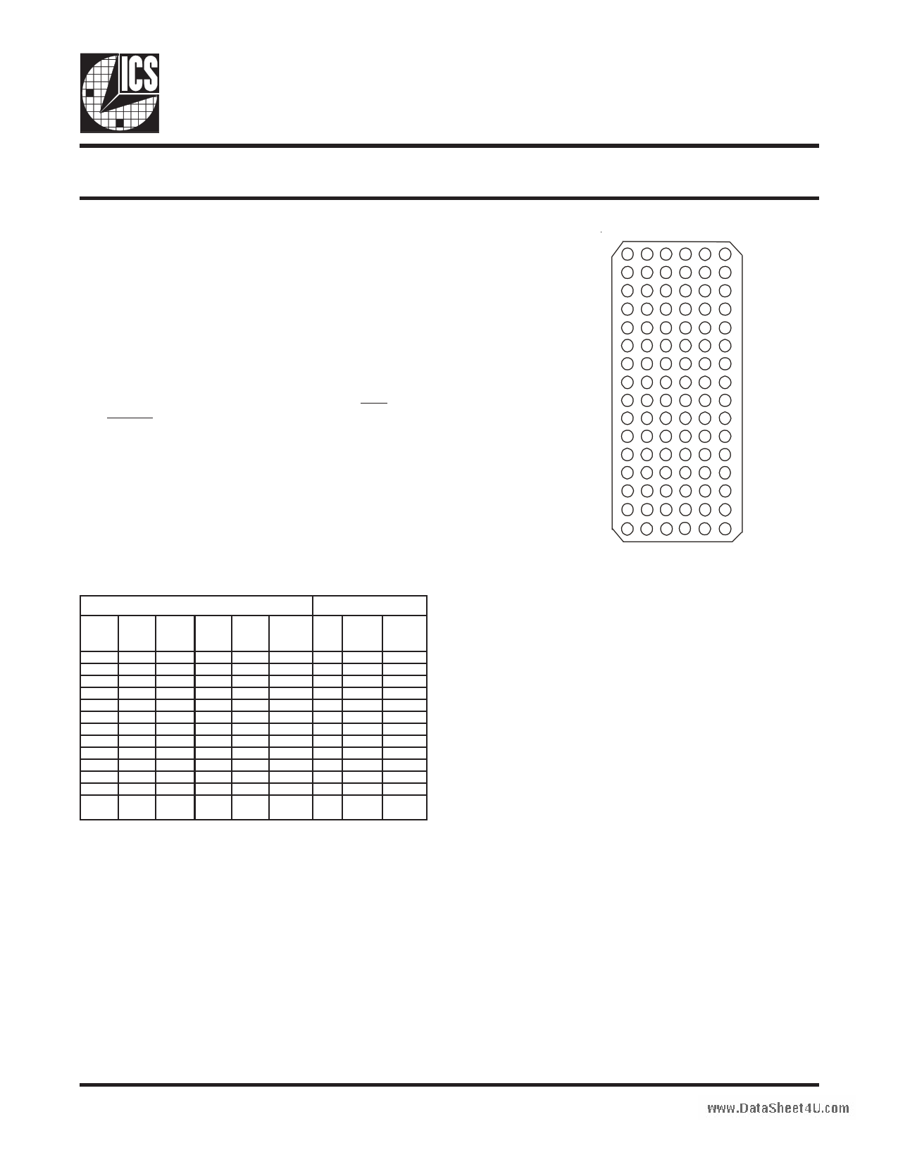
Pin Configuration
123456
A
B
C
D
E
F
G
H
J
K
L
M
N
P
R
T
96 Ball BGA
(Top View)
1165—10/25/06
ADVANCE INFORMATION documents contain information on products in the formative or design phase development. Characteristic data and other specifications are design goals.
ICS reserves the right to change or discontinue these products without notice. Third party brands and names are the property of their respective owners.
1 page 
Block Diagram for 1:1 mode (positive logic)
RST
CK
CK
VREF
DCKE
DODT
DCS
CSR
ICSSSTUB32866B
Advance Information
D
C1
R
D
C1
R
1D
C1
R
QCKEA
QOTDA
QCSA#
D1 O
1
1D
C1
R
Q1A
(1)
Q1B
1165—10/25/06
TO 21 OTHER CHANNELS
NOTE:
1. Disabled in 1:1 configuration.
5
5 Page 
ICSSSTUB32866B
Advance Information
2. Device standard (cont'd)
RST
DCS
CSR
n
n+1
n+2
n+3
n+4
CK
CK
D1•D25
Q1•Q25
PAR_IN
PPO
QERR †
tsu
tpdm , t pdmss
CK to
th
tsu th
tpd
CK to PPO
Data to PPO Latency
Data to QERR Latency
tPHL or t PLH
CK to QERR
Unknown input
event
Output signal is dependent on
the prior unknown input event
H or L
Figure 10
Timing diagram for SSTU32866 used as a single device; C0=0, C1=0;
RST being held high
† If the data is clocked in on the n clock pulse, the QERR output signal will be generated on the n+2 clock pulse, and it will be valid on
the n+3 clock pulse. If an error occurs and the QERR output is driven low, it stays latched low for a minimum of two clock cycles or
until RST is driven low.
1165—10/25/06
11
11 Page | ||
| Páginas | Total 28 Páginas | |
| PDF Descargar | [ Datasheet ICSSSTUB32866B.PDF ] | |
Hoja de datos destacado
| Número de pieza | Descripción | Fabricantes |
| ICSSSTUB32866B | 25-Bit Configurable Registered Buffer | ICS |
| Número de pieza | Descripción | Fabricantes |
| SLA6805M | High Voltage 3 phase Motor Driver IC. |
Sanken |
| SDC1742 | 12- and 14-Bit Hybrid Synchro / Resolver-to-Digital Converters. |
Analog Devices |
|
DataSheet.es es una pagina web que funciona como un repositorio de manuales o hoja de datos de muchos de los productos más populares, |
| DataSheet.es | 2020 | Privacy Policy | Contacto | Buscar |