|
|
|
PDF GS1515 Data sheet ( Hoja de datos )
| Número de pieza | GS1515 | |
| Descripción | HDTV Serial Digital Reclocker | |
| Fabricantes | Gennum Corporation | |
| Logotipo | ||
Hay una vista previa y un enlace de descarga de GS1515 (archivo pdf) en la parte inferior de esta página. Total 17 Páginas | ||
|
No Preview Available !
www.DataSheet4U.com
HD-LINX ™ GS1515
HDTV Serial Digital Reclocker
FEATURES
• SMPTE 292M compliant
• fully automatic adjustment free reclocker for HDTV
signals
• 1.485Gb/s and 1.485/1.001Gb/s operation
• dual 75Ω co-axial cable driver outputs
• reclocker bypass mode
• seamless input Interface to the GS1504 HD adaptive
equalizer
• low power
• lock detect
• +5V or -5V power supply operation
• 44 pin MQFP
APPLICATIONS
SMPTE 292M Serial Digital Routers; SMPTE 292M Serial
Digital Distribution Amplifiers.
ORDERING INFORMATION
PART NUMBER
PACKAGE
GS1515-CQM
44 pin MQFP
GS1515-CTM
44 pin MQFP Tape
TEMPERATURE
0°C to 70°C
0°C to 70°C
DESCRIPTION
PRELIMINARY DATA SHEET
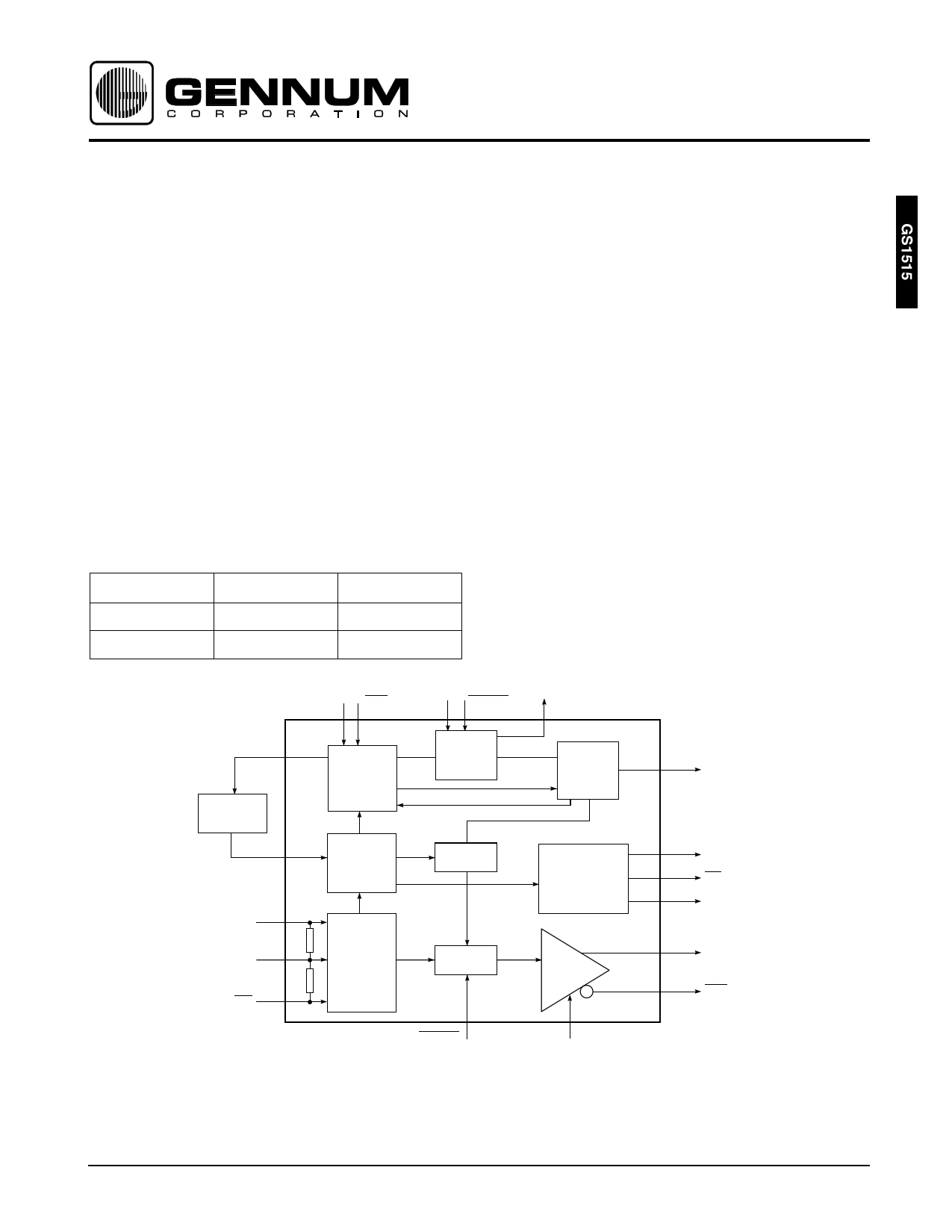
The GS1515 HDTV Serial Digital Reclocker is designed to
automatically recover the embedded clock signal and re-
time the data from a SMPTE 292M compliant digital video
signal.
An internal low pass filter removes the high frequency jitter
components from the bit-serial stream. 100Ω differential
input termination is on-chip for seamless matching to 50Ω
transmission lines. A dual SMPTE 292M compliant output
Cable Driver is also included on-chip. The GS1515 uses the
GO1515 external VCO connected to the internal PLL
circuitry in order to achieve ultra low noise PLL
performance.
Two diagnostic features are included in the GS1515 for
robust system design. The Input Jitter Indicator (IJI)
indicates excessive input jitter before the Serial Digital
outputs are muted and the Jitter Demodulator Function
(DM) helps to debug systems and locate the source of jitter.
The GS1515 is packaged in a 44 pin MQFP package and
requires a single 5V power supply. The GS1515 typically
draws 100mA of current.
LFS LFS PLCAP PLCAP
IJI
LFA
GO1515
VCO
VCO
CHARGE
PUMP
PHASE
DETECTOR
PHASE
LOCK
MUTE
LOGIC
JITTER
DEMODULATOR
DDI
DDI_VTT
DDI
50
INPUT
BUFFER
50
PATENT PENDING
BYPASS
BYPASS
CABLE
DRIVER
RSET
BLOCK DIAGRAM
PLL_LOCK
DM
DM
DFT_VEE
SDO
SDO
Revision Date: January 2000
Document No. 522 - 23 - 01
GENNUM CORPORATION P.O. Box 489, Stn. A, Burlington, Ontario, Canada L7R 3Y3
Tel. +1 (905) 632-2996 Fax. +1 (905) 632-5946 E-mail: [email protected]
www.gennum.com
1 page 
PIN DESCRIPTIONS
NUMBER
SYMBOL
1, 3, 4, 6, 7, 9, 10,
24, 25, 27, 29, 31,
33, 34, 36, 38
NC
2 LFS
5 LFA_VEE
8 LFA_VCC
11 LFA
12 DFT_VEE
13, 14
15, 18, 22
PLCAP,
PLCAP
SHIELD
16, 17
19
20, 21
23
26
28
30
32
35, 37
39, 40
41
42
VCO, VCO
DDI_VTT
DDI, DDI
PD_VCC
PD_VEE
CD_VEE
RSET
CD_VCC
SDO, SDO
DM, DM
IJI
PLL_LOCK
43 BYPASS
44 LFS
TYPE
DESCRIPTION
No connection. These pins are not bonded to the die.
INPUT
POWER
POWER
OUTPUT
POWER
INPUT
Loop filter capacitor connection.
Most negative power supply connection - loop filter circuitry.
Most positive power supply connection - loop filter circuitry.
Control signal output: control voltage for the external GO1515 VCO.
Most negative power supply connection - that enables the jitter demodulator
functionality, this pin should be connected to ground. If left floating, the DM
function is disabled resulting in a current saving of 340µA.
Control signal input: PLL lock detect time constant capacitor connection.
INPUT
INPUT
INPUT
POWER
POWER
POWER
INPUT
POWER
OUTPUT
OUTPUT
OUTPUT
OUTPUT
INPUT
INPUT
No connect pins separating the DDI inputs, the VCO inputs and the loop filter
components to improve noise performance. Connection to be made to ground
in most cases depending upon PCB performance.
Control signal inputs: differential inputs for the external VCO. The GO1515 has
single ended output. In this case, the VCO input is decoupled to ground.
Centre tap of the two 50Ω on-chip termination resistors between the DDI and
the DDI inputs.
Differential inputs for the serial digital signals.
Most positive power supply connection - phase detector circuitry.
Most negative poser supply connection - phase detector circuitry.
Most negative power supply connection - cable driver circuitry.
Resistor used to set the serial digital output signal swing. It is connected
between here and ground with a very short trace length.
Most positive power supply connection - cable driver circuitry.
Differential serial digital outputs from the on-chip cable driver. These outputs
require 75Ω pull-up resistors.
Diagnostic signal: if the jitter demodulator function is not used, these pins must
be left floating.
Status signal output: indicates the amount of excessive jitter on the incoming
DDI and DDI signals.
Status signal output: lock detect and carrier detect: PLL lock indicator output
used to indicate when the PLL is locked. This output is TTL compatible. When
the PLL_LOCK = LOW, the serial digital outputs are muted.
Control signal input: operational TTL compatible input that controls whether the
input DDI and DDI signal is reclocked (BYPASS = HIGH) or is passed through
the device, unreclocked (BYPASS = LOW). Muting does not affect the
bypassed signal.
Loop filter capacitor connection.
5
522 - 23 - 01
5 Page 
PHASE LOCK
The phase lock circuit is used to determine the phase
locked condition. It is done by generating a quadrature
clock by delaying the in-phase clock (the clock whose
falling edge is aligned to the data transition) by 166ps
(0.25UI at 1.5GHz) with the tolerance of 0.05UI. When the
PLL is locked, the falling edge of the in-phase clock is
aligned with the data edges as shown in Figure 18. The
quadrature clock is in a logic high state in the vicinity of
input data transitions. The quadrature clock is sampled and
latched by positive edges of the data transitions. The
generated signal is low pass filtered with an RC network.
The R is an on-chip 20kΩ resistor and CPL is an external
capacitor (recommended value 10nF). The time constant is
about 67µs, or more than a video line.
PHASE ALIGNMENT
EDGE
IN-PHASE CLOCK
RE-TIMING
EDGE
INPUT DATA
WITH JITTER
0.25UI
QUADERATURE
CLOCK
0.8UI
average of the ratio of the transitions inside the quadrature
clock and outside the quadrature is available at the PLCAP/
PLCAP pins. A signal, IJI, which is the buffered signal
available at the PLCAP is provided so that loading does not
effect the filter circuit. The signal at IJI is referenced with the
power supply such that the factor VIJI/VCC is a constant over
process and power supply for a given input jitter
modulation. The IJI signal has 10kΩ output impedance.
Figure 19 shows the relationship of the IJI signal with
respect to the sine wave modulated input jitter.
P-P SINE WAVE JITTER IN UI
0.00
0.15
0.30
0.39
0.45
0.48
0.52
0.55
0.58
0.60
0.63
IJI VOLTAGE
4.75
4.75
4.75
4.70
4.60
4.50
4.40
4.30
4.20
4.10
3.95
PLCAP SIGNAL
PLCAP SIGNAL
Fig. 18 PLL Circuit Principles
If the signal is not locked, the data transition phase could
be anywhere with respect to the internal clock or the
quadrature clock. In this case, the normalized filtered
sample of the quadrature clock will be 0.5. When VCO is
locked to the incoming data, data will only sample the
quadrature clock when it is logic high. The normalized
filtered sample quadrature clock will be 1.0. We chose a
threshold of 0.66 to generate the phase lock signal.
Because the threshold is lower than 1, it allows jitter to be
bigger than 0.5UI before the phase lock circuit reads it as
“not phase locked”.
INPUT JITTER INDICATOR (IJI)
This signal indicates the amount of excessive jitter (beyond
the quadrature clock window 0.5UI), which occurs beyond
the quadrature clock window (see Figure 18). All the input
data transitions occurring outside the quadrature clock
window, will be captured and filtered by the low pass filter
as mentioned in the Phase Lock section. The running time
5.0
4.8
4.6
4.4
4.2
4.0
3.8
3.6
0.00
0.20
0.40
0.60
INPUT JITTER (UI)
0.80
Fig. 19 Input Jitter Indicator (Typical at TA = 25°C)
LOCK LOGIC
Logic is used to produce the PLL_LOCK signal which is
based on the LFS signal and phase lock signal. When there
is not any data input, the integrator will charge and
eventually saturate at either end. By sensing the saturation
of the integrator, it is determined that no data is present. If
either data is not present or phase lock is low, the lock
signal is made low. Logic signals are used to acquire the
frequency by sweeping the integrator. Injecting a current
11
522 - 23 - 01
11 Page | ||
| Páginas | Total 17 Páginas | |
| PDF Descargar | [ Datasheet GS1515.PDF ] | |
Hoja de datos destacado
| Número de pieza | Descripción | Fabricantes |
| GS1510 | HDTV Serial Digital Deformatter | Gennum Corporation |
| GS1511 | HD-LINX -TM GS1511 HDTV Serial Digital Formatter | Gennum Corporation |
| GS1515 | HDTV Serial Digital Reclocker | Gennum Corporation |
| Número de pieza | Descripción | Fabricantes |
| SLA6805M | High Voltage 3 phase Motor Driver IC. |
Sanken |
| SDC1742 | 12- and 14-Bit Hybrid Synchro / Resolver-to-Digital Converters. |
Analog Devices |
|
DataSheet.es es una pagina web que funciona como un repositorio de manuales o hoja de datos de muchos de los productos más populares, |
| DataSheet.es | 2020 | Privacy Policy | Contacto | Buscar |