|
|
|
PDF DS2704 Data sheet ( Hoja de datos )
| Número de pieza | DS2704 | |
| Descripción | 1280-Bit EEPROM | |
| Fabricantes | Maxim Integrated Products | |
| Logotipo | ||
Hay una vista previa y un enlace de descarga de DS2704 (archivo pdf) en la parte inferior de esta página. Total 18 Páginas | ||
|
No Preview Available !
www.DataSheet4U.com
DS2704
1280-Bit EEPROM with SHA-1 Authentication
www.maxim-ic.com
GENERAL DESCRIPTION
The DS2704 provides 1280 bits of EEPROM data
storage and a Secure Hash Algorithm (SHA) engine.
The Dallas 1-WireÒ interface enables serial
communication on a single battery contact and the
64-bit unique serial number allows multidrop
networking and identification of individual devices.
The 1280-bit memory is organized as 5 pages of 32
bytes each and supports storage of battery cell
characteristics, charging voltage, current, and
temperature parameters, as well as battery pack
manufacturing data. The EEPROM pages are in
circuit rewritable and can be individually locked to
write protect data.
The DS2704 employs the Secure Hash Algorithm
(SHA-1) specified in the Federal Information
publication 180-1 and 180-2, and ISO/IEC 10118-3.
SHA-1 provides a robust cryptographic solution to
ensure battery packs or other peripherals have been
manufactured by authorized sources. The DS2704
processes a host transmitted challenge and the 64-
bit secret key stored on chip to produce a 160-bit
response for transmission back to the host. The
secret key is never transmitted between the battery
and the host.
APPLICATION EXAMPLE
PACK+
150W
DATA
150W
THM
V DD
DQ
DS2704
4.7V
VSS
PACK-
0.01mF
Li+
Safety
Circuit
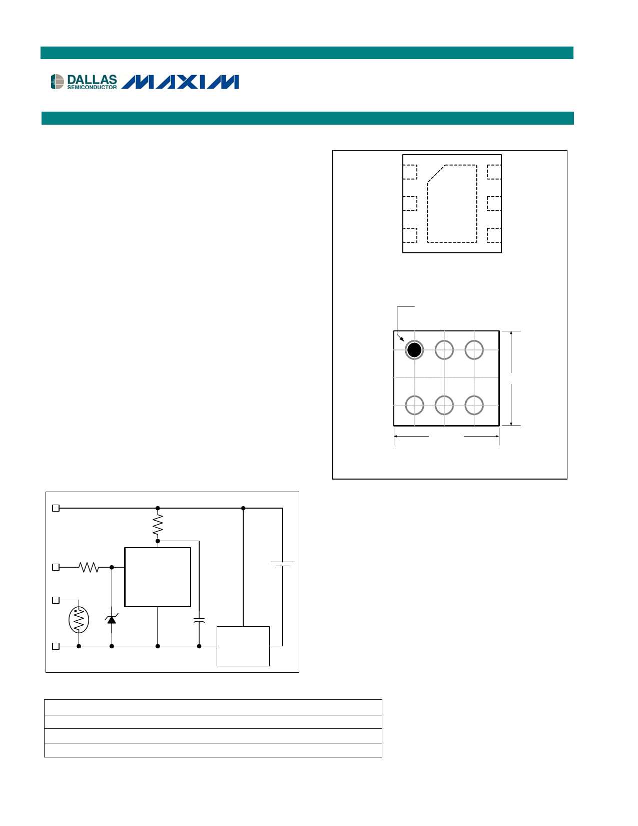
PIN CONFIGURATION
VDD 1
6 DQ
NC 2
5 VSS
NC 3
4 NC
3mm × 3mm TDFN
(TOP VIEW¾PADS ON BOTTOM)
Top Side A1 Mark
12 3
A
B 1.73
C
1.98 mm
UCSP (FUTURE AVAILABILITY)
(TOP VIEW¾BALLS ON BOTTOM)
FEATURES
§ Secure Challenge and Response Authentication
Using the SHA-1 Algorithm
§ Five Lockable 32-Byte Pages of EEPROM
§ Dallas 1-Wire Interface with Standard and
Overdrive Communications Speeds
§ Unique 64-Bit Serial Number
§ Compatible with DS2502 Memory Map and Read
Function Command
§ Operates with VDD as Low as 2.5V
§ Tiny Chip-Scale UCSP and 3mm x 3mm TDFN
Packaging (Pb-free)
ORDERING INFORMATION
PART
TEMP RANGE
DS2704G+
-20°C to +70°C
DS2704G+T&R
DS2704W
-20°C to +70°C
-20°C to +70°C
PIN-PACKAGE
6-TDFN
DS2704G+ on Tape-and-Reel
Bare Die
+ Denotes lead-free package.
1-Wire is a registered trademark of Dallas Semiconductor.
1 of 18
011206
1 page 
DS2704: 1280-Bit EEPROM with SHA-1 Authentication
Programming mode is entered when writing the nonvolatile memory portions of the DS2704. The supply current
increases to IDDP for tEEC when a Copy Scratchpad, Write Status, Compute Secret, Clear/Lock Secret or Clear/Set
Overdrive Timing command is executed.
Functional compatibility has been maintained between the DS2502 and DS2704 at the Net Address/ROM
Command and Function Command levels for reading the Memory and Status data fields. Since the DS2704 is
based on EEPROM technology versus the EPROM technology used for the DS2502, writing of the Memory and
Status data fields is not the same as the DS2502. The DS2704 includes an on-chip charge pump to facilitate in-
circuit programming. The need to apply an external high voltage programming pulse during pack manufacture is
therefore eliminated. Data can be written to a 0 or 1 value up to NEEC times in the DS2704. The ability to reprogram
the data in the EEPROM pages makes the Page Address Redirection bytes in the Status data field unnecessary.
Therefore, the DS2704 maintains them for DS2502 read compatibility but they cannot be modified from their factory
default values of FFh.
AUTHENTICATION
Authentication is performed using a FIPS-180 compliant SHA-1 one way hash algorithm on a 512-bit message
block. The message block consists of a 64-bit secret, a 64-bit challenge and 384 bits of constant data. Optionally,
the 64-bit net address replaces 64 of the 384 bits of constant data used in the hash operation. Contact
Dallas/Maxim for details of the message block organization.
The host and the DS2704 both calculate the result based on the mutually known secret. The result data, known as
the Message Authentication Code (MAC) or Message Digest, is returned by the DS2704 for comparison to the
host’s result. Note that the secret is never transmitted on the bus and thus cannot be captured by observing bus
traffic. Each authentication attempt is initiated by the host system by providing a 64-bit random challenge via the
Write Challenge command. The host then issues the Compute MAC or Compute MAC with ROM ID command. The
MAC is computed per FIPS 180, and then returned as a 160-bit serial stream, beginning with the least significant
bit.
DS2704 AUTHENTICATION COMMANDS
WRITE CHALLENGE [0Ch]. This command writes the 64-bit challenge to the DS2704. The LSB of the 64-bit data
argument can begin immediately after the MSB of the command has been completed. If more than 8 bytes are
written, the final value in the challenge register will be indeterminate. The Write Challenge command must be
issued prior to every Compute MAC or Compute Next Secret command for reliable results.
COMPUTE MAC WITHOUT ROM ID [36h]. This command initiates a SHA-1 computation based on the Challenge
value and internal Secret. Logical 1’s are loaded in place of the ROM ID. This command allows the use of a master
secret and MAC response independent of the ROM ID. The DS2704 computes the MAC in tSHA after receiving the
last bit of this command. After the MAC computation is complete, the host must write 8 write zero time slots and
then issue 160 read time slots to receive the 20-byte MAC. See Figure 7 on page 16 for command timing.
COMPUTE MAC WITH ROM ID [35h]
This command is structured the same as the Compute MAC without ROM ID, except that the ROM ID is included in
the message block. With the ROM ID unique to each DS2704 included in the MAC computation, use of a unique
secret in each token and a master secret in the host device is allowed. See application note “White Paper 4”,
available at http://www.maxim-ic.com, for more information. See Figure 7 on page 16 for command timing.
NOTE: Immediately after power-up, a dummy Compute MAC command is required to initialize the DS2704. If the
dummy command is not issued, the first authentication attempt is computed using a challenge value of 0. When
issuing the dummy Compute MAC command, the command sequence can be terminated immediately following the
8th bit of the Compute MAC command byte. Waiting for the SHA-1 computation and reading the results back are
not required.
SHA-1 related commands used while authenticating a battery or peripheral device are summarized in Table 1 for
convenience. Four additional commands for clearing, computing and locking of the Secret are described in detail in
the following section.
5 of 18
5 Page 
CRC GENERATION
DS2704: 1280-Bit EEPROM with SHA-1 Authentication
The DS2704 has an 8-bit CRC stored in the most significant byte of its 1-Wire net address and generates a CRC
during some command protocols. To ensure error-free transmission of the address, the host system can compute a
CRC value from the first 56 bits of the address and compare it to the CRC from the DS2704.
The host system is responsible for verifying the CRC value and taking action as a result. The DS2704 does not
compare CRC values and does not prevent a command sequence from proceeding as a result of a CRC mismatch.
Proper use of the CRC can result in a communication channel with a very high level of integrity.
The CRC can be generated by the host using a circuit consisting of a shift register and XOR gates as shown in
Figure 3, or it can be generated in software using the polynomial X8 + X5 + X4 + 1. Additional information about the
Dallas 1-Wire CRC is available in Application Note 27: Understanding and Using Cyclic Redundancy Checks with
Dallas Semiconductor Touch Memory Products (www.maxim-ic.com/appnoteindex).
In the circuit in Figure 3, the shift register bits are initialized to 0. Then, starting with the least significant bit of the
family code, one bit at a time is shifted in. After the 8th bit of the family code has been entered, then the serial
number is entered. After the 48th bit of the serial number has been entered, the shift register contains the CRC
value.
Figure 3. 1-Wire CRC Generation Block Diagram
MSb
XOR
XOR
INPUT
LSb
XOR
During some command sequences, the DS2704 also generates an 8-bit CRC and provides this value to the bus
master to facilitate validation for the transfer of command, address, and data from the bus master to the DS2704.
The DS2704 computes an 8-bit CRC for the command and address bytes received from the bus master for the
Read Memory, Read Status and Read/Generate CRC commands to confirm that these bytes have been received
correctly. The CRC generator on the DS2704 is also used to provide verification of error-free data transfer as each
EEPROM page is sent to the master during a Read Data/Generate CRC command and for the 8 bytes of
information in the Status memory field.
In each case where a CRC is used for data transfer validation, the bus master must calculate the CRC value using
the same polynomial function and compare the calculated value to the CRC either stored in the DS2704 Net
Address or computed by the DS2704. The comparison of CRC values and decision to continue with an operation
are determined entirely by the bus master. There is no circuitry in the DS2704 that prevents the a command
sequence from proceeding if the stored or calculated CRC from the DS2704 and the calculated CRC from the host
do not match.
HARDWARE CONFIGURATION
Because the 1-Wire bus has only a single line, it is important that each device on the bus be able to drive it at the
appropriate time. To facilitate this, each device attached to the 1-Wire bus must connect to the bus with open-drain
or tri-state output drivers. The DS2704 uses an open-drain output driver as part of the bidirectional interface
circuitry shown in Figure 4. If a bidirectional pin is not available on the bus master, separate output and input pins
can be connected together.
The 1-Wire bus must have a pullup resistor at the bus-master end of the bus. A value of between 2kW and 5kW is
recommended. The idle state for the 1-Wire bus is high. If, for any reason, a bus transaction must be suspended,
the bus must be left in the idle state to properly resume the transaction later. Note that if the bus is left low for more
than tRSTL, slave devices on the bus begin to interpret the low period as a reset pulse, effectively terminating the
transaction.
11 of 18
11 Page | ||
| Páginas | Total 18 Páginas | |
| PDF Descargar | [ Datasheet DS2704.PDF ] | |
Hoja de datos destacado
| Número de pieza | Descripción | Fabricantes |
| DS2703 | SHA-1 Battery Pack Authentication IC | Dallas Semiconductor |
| DS2704 | 1280-Bit EEPROM | Maxim Integrated Products |
| DS2705 | SHA-1 Authentication Master | Maxim Integrated Products |
| Número de pieza | Descripción | Fabricantes |
| SLA6805M | High Voltage 3 phase Motor Driver IC. |
Sanken |
| SDC1742 | 12- and 14-Bit Hybrid Synchro / Resolver-to-Digital Converters. |
Analog Devices |
|
DataSheet.es es una pagina web que funciona como un repositorio de manuales o hoja de datos de muchos de los productos más populares, |
| DataSheet.es | 2020 | Privacy Policy | Contacto | Buscar |