|
|
PDF UPD121W1xxA Data sheet ( Hoja de datos )
| Número de pieza | UPD121W1xxA | |
| Descripción | MOS INTEGRATED CIRCUIT | |
| Fabricantes | NEC | |
| Logotipo |  |
|
Hay una vista previa y un enlace de descarga de UPD121W1xxA (archivo pdf) en la parte inferior de esta página. Total 16 Páginas | ||
|
No Preview Available !
www.DataSheet4U.com
DATA SHEET
MOS INTEGRATED CIRCUIT
μ PD121WxxA Series
HIGH CURRENT 1.5 A
GENERAL-PURPOSE CMOS REGULATOR
DESCRIPTION
The μ PD121WxxA series is general-purpose CMOS regulators which have 1.5 A output current capacity. These
products are suitable for power supply of large-scale ASICs etc. By ON/OFF function, the power consumption can be
kept low level at the time of off-state. This series of regulator has 3 fixed output voltage type 1.8 V, 2.5 V, 3.3 V, and
adjustable output voltage type (1.8 to 3.3 V).
FEATURES
• Output Current: 1.5 A
• Output Voltage: 1.8 V, 2.5 V, 3.3 V (Fixed type) / 1.8 to 3.3 V (Adjustable type)
• Output Voltage Tolerance: VO ± 2.0% (TJ = 25°C)
• Dropout Voltage: VDIF = 1.0 V MAX. (IO = 1.5 A)
• Quiescent Current: 150 μ A TYP. (IO = 0 A)
• Standby Current: 1 μ A
• Available for laminated ceramic capacitor: (Electric capacity 10 μ F or higher)
• On-chip over-current protection circuit
• On-chip thermal shut down circuit
APPLICATIONS
These regulators are suitable for large-scale ASICs which are used in digital appliances etc.
PIN CONFIGURATION (Marking Side)
5-PIN TO-252 (5-PIN MP-3ZK)
6
1 2 345
1. INPUT
2. ON/OFF
3. GND Note
4. NC / ADJ
5. OUTPUT
6. GND (Fin)
Note No.3 pin is cut and can not be connected to substrate. No.6 is Fin and common to GND pin.
The information in this document is subject to change without notice. Before using this document, please
confirm that this is the latest version.
Not all products and/or types are available in every country. Please check with an NEC Electronics
sales representative for availability and additional information.
Document No. G18852EJ1V0DS00 (1st edition)
Date Published July 2007 NS
Printed in Japan
2007
1 page 
μ PD121WxxA Series
CIN : 0.1 μ F or higher. Be sure to connect CIN to prevent parasitic oscillation. Set this value according to the length
of the line between the regulator and the INPUT pin. Use of a film capacitor or other capacitor with first-rate
voltage and temperature characteristics is recommended. If using a laminated ceramic capacitor, it is
necessary to ensure that CIN is 0.1 μ F or higher for the voltage and temperature range to be used.
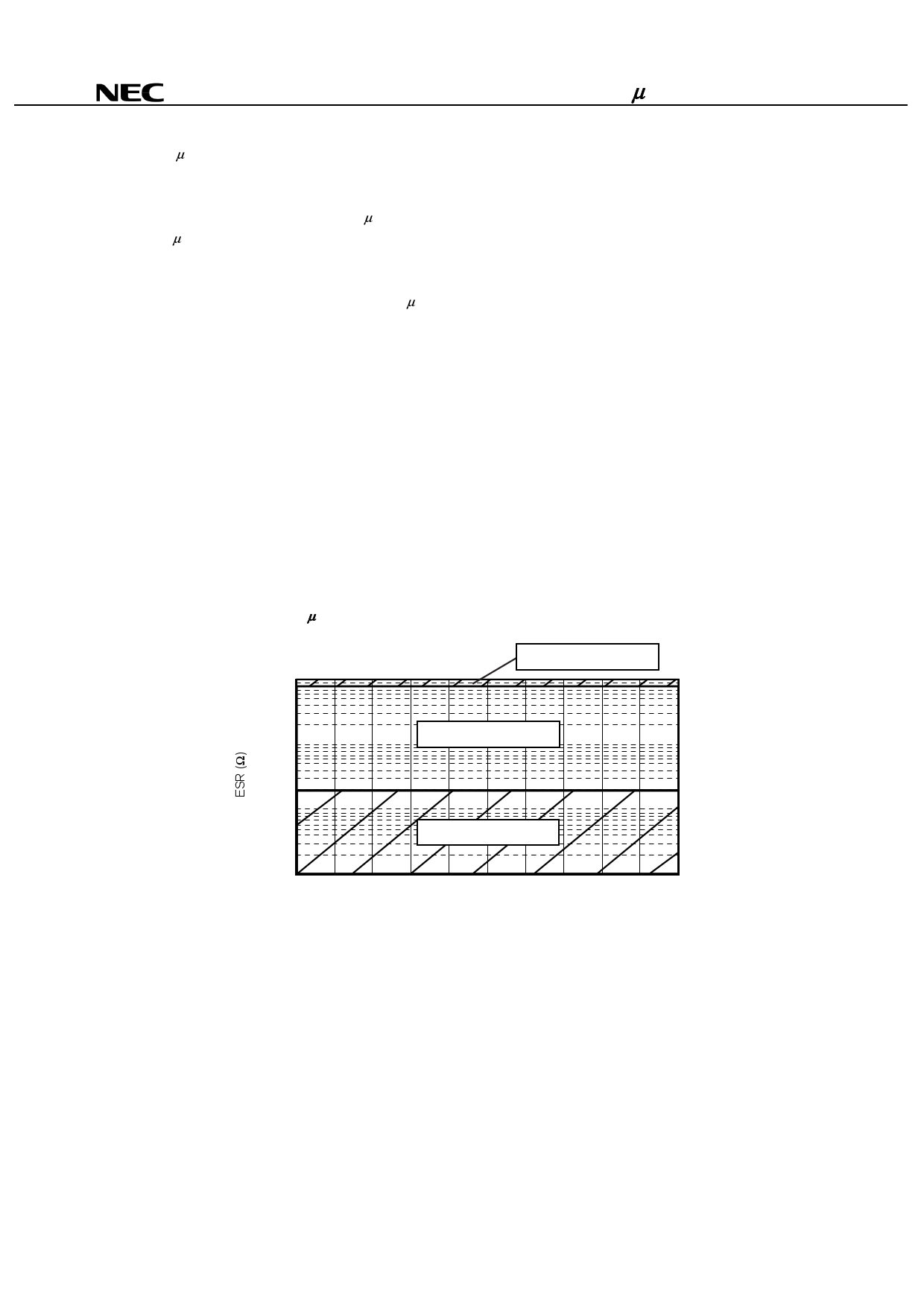
COUT : 10 μ F or higher. Be sure to connect COUT to prevent oscillation and improve excessive load regulation. Place
CIN and COUT as close as possible to the IC pins (within 1 to 2 cm). Also, in case of using a laminated ceramic
capacitor, please note following items.
• It is necessary to ensure that COUT is 10 μ F or higher for the voltage and temperature range to be used.
• In case of using laminated ceramic capacitor, it is easy to become state of parasitic oscillation. Because
ESR of laminated ceramic capacitor is very low. Therefore, the capacitor and load condition (output current)
which fulfill the condition of the stable operation area of ESR shown below are recommended.
• Stable Operation Area as below is regulated under condition of which this product is not on a substrate.
Therefore impedance on substrate is not considered.
D1 : If the OUTPUT pin has a higher voltage than the INPUT pin, connect a diode.
D2 : If the OUTPUT pin has a lower voltage than the GND pin, connect a Schottky barrier diode.
R1, R2: The total amount of R1 and R2 is sure to below 500 kΩ (375 kΩ TYP.). R2 = 100 kΩ is recommended.
VOUT = (1 + R1/R2) VADJ Note
Note When VOUT = 3.0 V: R1 = 275 kΩ, R2 = 100 kΩ
Caution Make sure that no external voltage is applied to the OUTPUT pin.
μ PD121WxxA Series COUT ESR Stable Operation Area
Unstable Operation Area
10
1 Stable Operation Area
0.1
Unstable Operation Area
0.01
0
150 300 450 600 750 900 1050 1200 1350 1500
IO (mA)
Data Sheet G18852EJ1V0DS
5
5 Page 
3.0
2.5
2.0
1.5
1.0
0.5
0
0
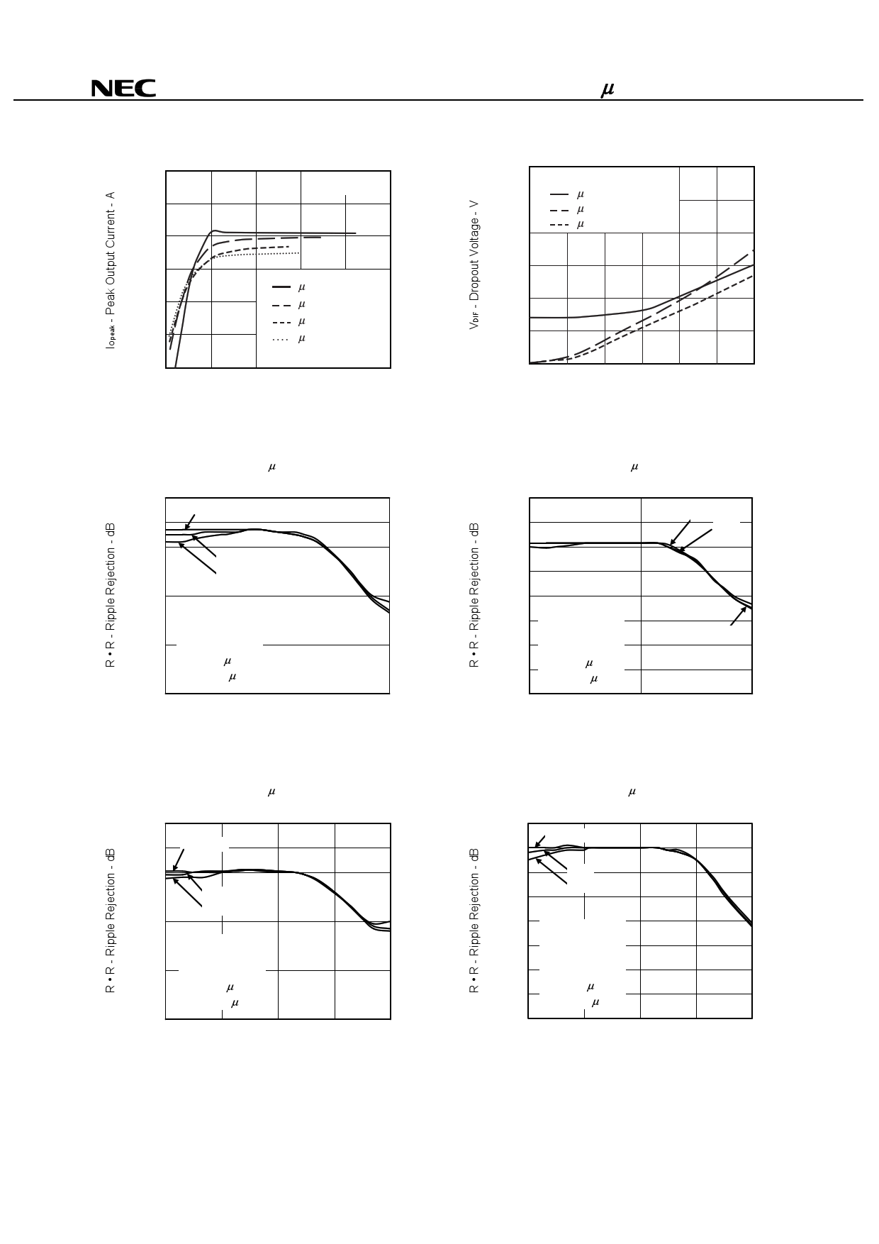
IOpeak vs. VDIF
TJ = 25°C
μ PD121W18A
μ PD121W25A
μ PD121W33A
μ PD121W00ANote
Note VO = 3.0 V
1.0 2.0 3.0 4.0 5.0
VDIF - Dropout Voltage - V
R • R vs. f ( μ PD121W18A)
80
IO = 5 mA
70
60
0.5 A
50 1.0 A
40
30 TJ = 25°C
VIN = 2.8 to 3.8 V
20 VON/OFF = 1.5 V
10
CIN = 0.1 μ F
COUT = 10 μ F
0
10 100
1k
10 k
f - Frequency - Hz
100 k
R • R vs. f (μ PD121W33A)
80
70 IO = 5 mA
60
50 0.5 A
1.0 A
40
30 TJ = 25°C
VIN = 4.3 to 5.3 V
20 VON/OFF = 1.5 V
10
CIN = 0.1 μ F
COUT = 10 μ F
0
10 100 1 k
10 k
f - Frequency - Hz
100 k
μ PD121WxxA Series
VDIF vs. IO
1.2
TJ = 25°C
1.0
μ PD121W18A
μ PD121W25A
0.8 μPD121W33A
0.6
0.4
0.2
0
0 0.25 0.5 0.75 1.0 1.25 1.5
IO - Output Current - A
R • R vs. f (μ PD121W25A)
80
70
60
50
40
30 TJ = 25°C
VIN = 3.5 to 4.5 V
20 VON/OFF = 1.5 V
10 CIN = 0.1 μ F
COUT = 10 μ F
0
10 100
1k
IO = 5 mA
0.5 A
1.0 A
10 k 100 k
f - Frequency - Hz
R • R vs. f (μ PD121W00A)
80
IO = 5 mA
70
60 0.5 A
1.0 A
50
40 TJ = 25°C
30 VO = 3.0 V
VIN = 4.0 to 5.0 V
20 VON/OFF = 1.5 V
10
CIN = 0.1 μ F
COUT = 10 μ F
0
10 100
1k
10 k
f - Frequency - Hz
100 k
Data Sheet G18852EJ1V0DS
11
11 Page | ||
| Páginas | Total 16 Páginas | |
| PDF Descargar | [ Datasheet UPD121W1xxA.PDF ] | |
Hoja de datos destacado
| Número de pieza | Descripción | Fabricantes |
| UPD121W1xxA | MOS INTEGRATED CIRCUIT | NEC |
| Número de pieza | Descripción | Fabricantes |
| SLA6805M | High Voltage 3 phase Motor Driver IC. |
Sanken |
| SDC1742 | 12- and 14-Bit Hybrid Synchro / Resolver-to-Digital Converters. |
Analog Devices |
|
DataSheet.es es una pagina web que funciona como un repositorio de manuales o hoja de datos de muchos de los productos más populares, |
| DataSheet.es | 2020 | Privacy Policy | Contacto | Buscar |
