|
|
|
PDF UPD121A10 Data sheet ( Hoja de datos )
| Número de pieza | UPD121A10 | |
| Descripción | MOS INTEGRATED CIRCUIT | |
| Fabricantes | NEC | |
| Logotipo | ||
Hay una vista previa y un enlace de descarga de UPD121A10 (archivo pdf) en la parte inferior de esta página. Total 10 Páginas | ||
|
No Preview Available !
www.DataSheet4U.com
DATA SHEET
MOS INTEGRATED CIRCUIT
μ PD121A10
2-POWER SUPPLY INPUT METHOD
1.0 V/2.0 A REGULATOR
DESCRIPTION
μ PD121A10 is the CMOS regulator which can output 2.0 A current. This regulator is suitable for power supply for 1.0
V ASIC core, for example our companies’ CB-90 (90 nm process LSI) etc. The dropout voltage is made small (0.7 V
MAX. (IO = 1.0 A) by dividing bias voltage (VDD) from input voltage (VIN). Therefore this product can output under the
conditions, VIN ≥ 1.62 V (VDD ≥ 4.0 V). Output voltage can be adjustable between 0.95 and 1.15 V.
FEATURES
• Output Current: 2.0 A
• Output Voltage: 0.95 to 1.15 V
• Bias Voltage: 4.0 to 5.5 V
• Reference Voltage Tolerance: VREF ± 10 mV (TJ = 25°C)
• Low Dropout Voltage: VDIF = 0.7 V MAX. (IO = 1.0 A)
• On-chip over-current protection circuit
• On-chip thermal shut down circuit
APPLICATIONS
This regulator is suitable for low power supply voltage IC,
for example core of CB-90 (90 nm process LSI) etc.
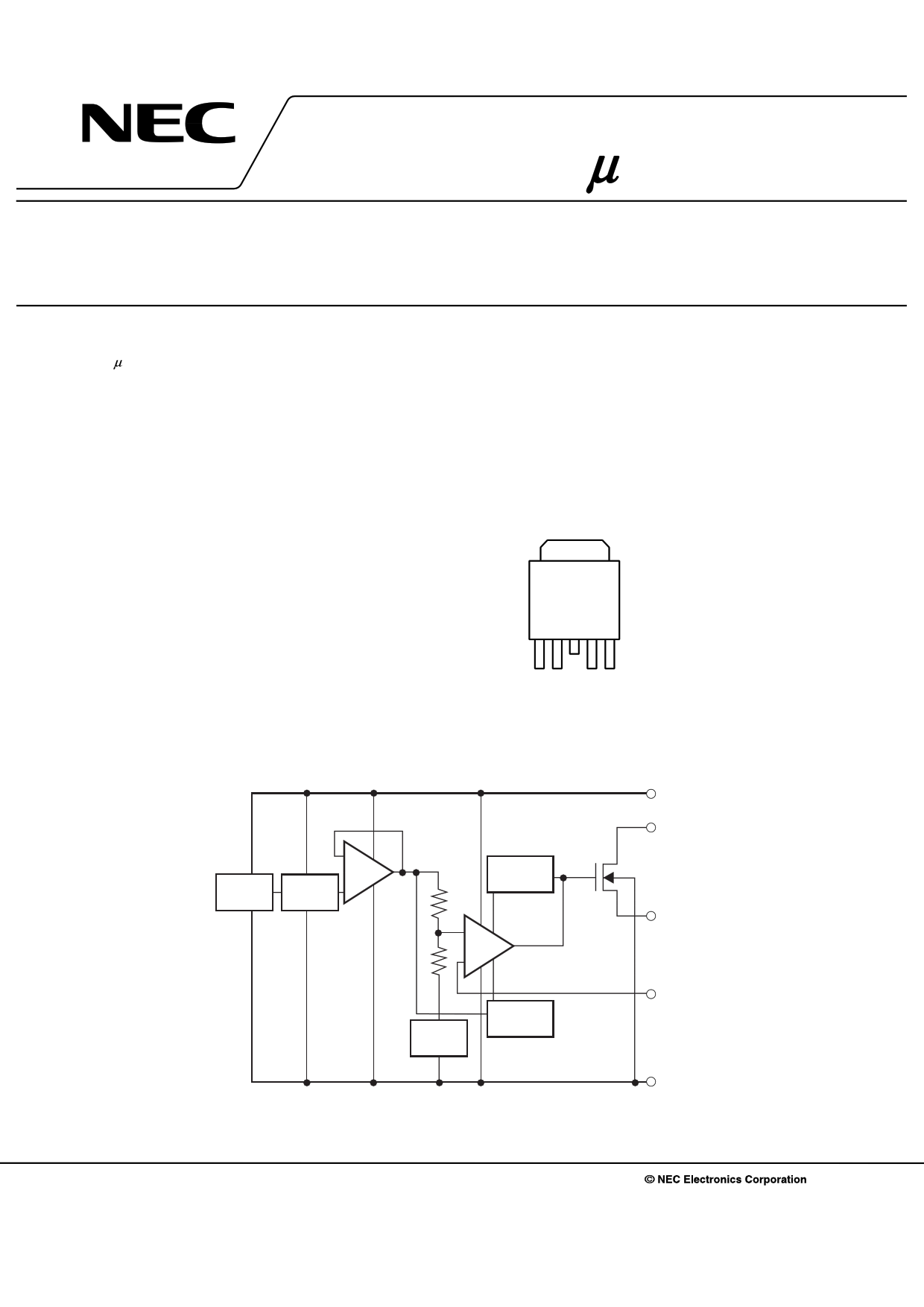
BLOCK DIAGRAM
PIN CONFIGURATION (Marking Side)
5-PIN TO-252 (5-PIN MP-3ZK)
6
1 2 345
1. INPUT
2. VDD (ON/OFF)
3. GND Note
4. SENSE
5. OUTPUT
6. GND (Fin)
Note No.3 pin is cut and can not be connected to
substrate. No.6 is Fin and common to GND pin.
Constant
current
Reference
voltage
−
Buffer
+
Over-current
protection
+
Error
amp.
−
Triming
Thermal
shut down
VDD
INPUT
OUTPUT
SENSE
GND
The information in this document is subject to change without notice. Before using this document, please
confirm that this is the latest version.
Not all products and/or types are available in every country. Please check with an NEC Electronics
sales representative for availability and additional information.
Document No. G18843EJ1V0DS00 (1st edition)
Date Published July 2007 NS
Printed in Japan
2007
1 page 
TYPICAL CHARACTERISTICS
PD vs. TA
20
15
10 With infinite heatsink
5
1.0
0
0
Without heatsink
50 85 100
150
TA - Operating Ambient Temperature - °C
μ PD121A10
10.0
5.0
Δ VREF vs.TJ
VIN = 2.0 V
VDD = 5.0 V
IO = 1.0 A
0
-5.0
-10.0
-20 0
25 50 75 100 125
TJ - Operating Junction Temperature - °C
VO vs. VDD
1.2
1.0
0.8
IO = 0 A
0.6
0.1 A
1.0 A
0.4
0.2
0
0
TJ = 25°C
VIN = 2.0 V
1.0 2.0 3.0 4.0 5.0
VDD - Bias Voltage - V
6.0
200
IBIAS vs. VDD
150
IO = 0 A
100
0.1 A
1.0 A
50
0
0
TJ = 25°C
VIN = 2.0 V
1.0 2.0 3.0 4.0 5.0
VDD - Bias Voltage - V
6.0
VDIF vs. TJ
0.3
0.25
0.2
0.15
0.1
0.05
0
-20 0
VDD = 5.0 V
IO = 1.0 A
25 50 75 100 125
TJ - Operating Junction Temperature - °C
R • R vs. f
80
70
IO = 0 A
60
50
40
30 TJ = 25°C
VIN = 1.8 to 2.2 V
20 VDD = 5.0 V
10
CIN = 0.1 μ F
COUT = 10 μ F
0
10
100
1k
1.0 A
2.0 A
10 k
f - Frequency - Hz
100 k
Data Sheet G18843EJ1V0DS
5
5 Page | ||
| Páginas | Total 10 Páginas | |
| PDF Descargar | [ Datasheet UPD121A10.PDF ] | |
Hoja de datos destacado
| Número de pieza | Descripción | Fabricantes |
| UPD121A10 | MOS INTEGRATED CIRCUIT | NEC |
| Número de pieza | Descripción | Fabricantes |
| SLA6805M | High Voltage 3 phase Motor Driver IC. |
Sanken |
| SDC1742 | 12- and 14-Bit Hybrid Synchro / Resolver-to-Digital Converters. |
Analog Devices |
|
DataSheet.es es una pagina web que funciona como un repositorio de manuales o hoja de datos de muchos de los productos más populares, |
| DataSheet.es | 2020 | Privacy Policy | Contacto | Buscar |