|
|
|
PDF RF5152 Data sheet ( Hoja de datos )
| Número de pieza | RF5152 | |
| Descripción | LINEAR POWER AMPLIFIER | |
| Fabricantes | RF Micro Devices | |
| Logotipo | ||
Hay una vista previa y un enlace de descarga de RF5152 (archivo pdf) en la parte inferior de esta página. Total 10 Páginas | ||
|
No Preview Available !
www.DataSheet4U.com
RF5152
3V TO 3.6V, 2.4GHz TO 2.5GHz
LINEAR POWER AMPLIFIER
Package Style: QFN, 16-Pin, 3 mm x 3 mm
Features
Single Power Supply 3.0V to
3.6 V
34dB Typical Small Signal Gain
50Ω Input and Interstage Match-
ing
2400MHz to 2500MHz Fre-
quency Range
+18dBm, 2.5%EVM (typ.),
130 mA@VCC = 3.3 V
Applications
IEEE802.11b/g/n WLAN Applica-
tions
2.5GHz ISM Band Applications
Commercial and Consumer Sys-
tems
Portable Battery-Powered Equip-
ment
Spread-Spectrum and MMDS
Systems
16 15 14 13
NC 1
12
RF OUT/
VC3
RF IN 2
Match
RF IN 3
NC 4
5
Match
Bias
6
Match
11 RF OUT
10 RF OUT
9 PDETECT
78
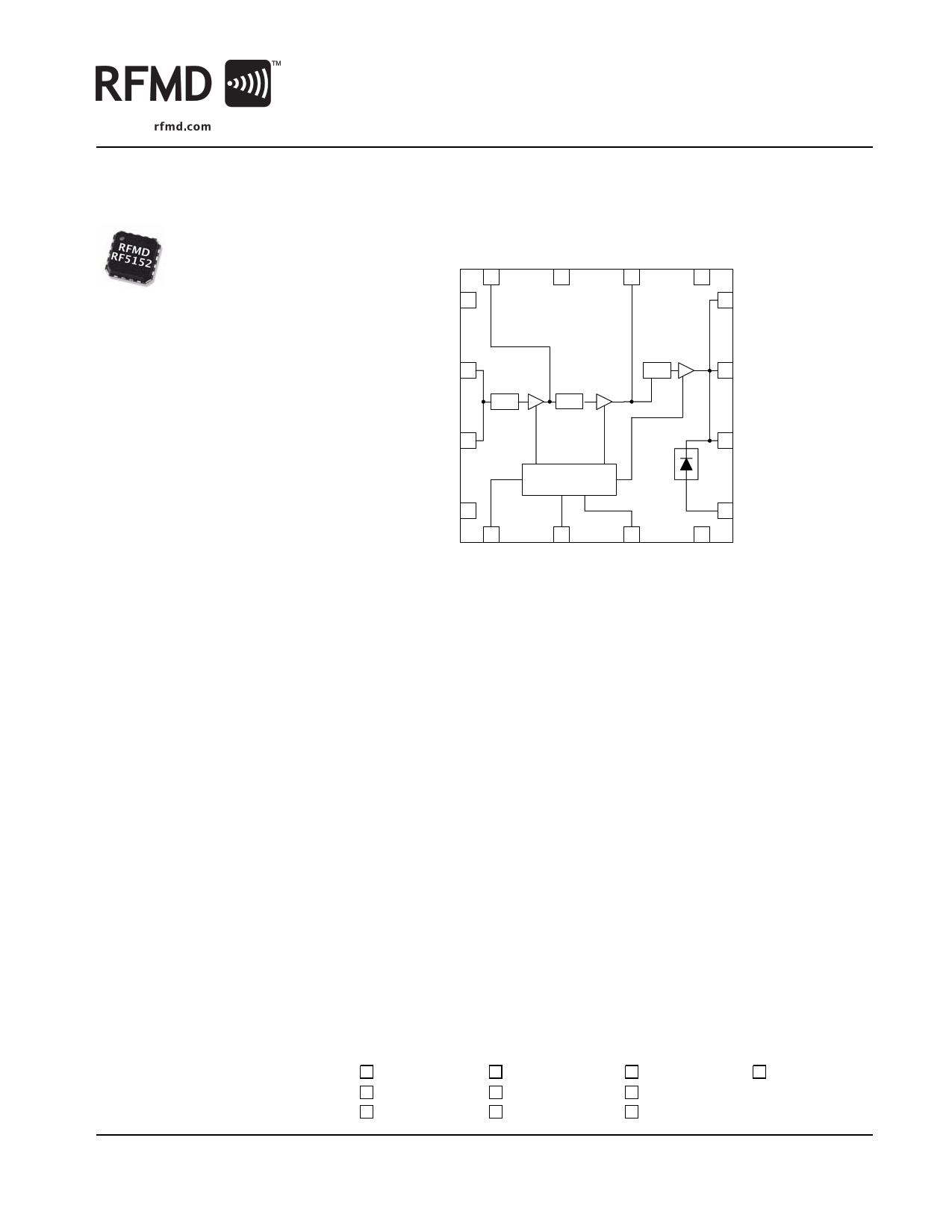
Functional Block Diagram
Product Description
The RF5152 is a linear, medium-power, high-efficiency, three-stage amplifier IC
designed specifically for battery-powered WLAN applications such as PC cards, mini
PCI, and compact flash applications. The device is manufactured on an advanced
InGaP Gallium Arsenide Heterojunction Bipolar Transistor (HBT) process, and has
been designed for use as the final RF amplifier in 2.5GHz OFDM and other spread-
spectrum transmitters. The device is provided in a 3mmx3mm, 16-pin, QFN with a
backside ground. The RF5152 is designed to maintain linearity over a wide range of
supply voltages and power outputs.
Ordering Information
RF5152
3V to 3.6V, 2.4GHz to 2.5GHz Linear Power Amplifier
RF5152PCBA-41X Fully Assembled Evaluation Board
Optimum Technology Matching® Applied
GaAs HBT
9GaAs MESFET
InGaP HBT
SiGe BiCMOS
Si BiCMOS
SiGe HBT
GaAs pHEMT
Si CMOS
Si BJT
GaN HEMT
RF MICRO DEVICES®, RFMD®, Optimum Technology Matching®, Enabling Wireless Connectivity™, PowerStar®, POLARIS™ TOTAL RADIO™ and UltimateBlue™ are trademarks of RFMD, LLC. BLUETOOTH is a trade-
mark owned by Bluetooth SIG, Inc., U.S.A. and licensed for use by RFMD. All other trade names, trademarks and registered trademarks are the property of their respective owners. ©2006, RF Micro Devices, Inc.
Rev A10 DS061221
7628 Thorndike Road, Greensboro, NC 27409-9421 · For sales or technical
support, contact RFMD at (+1) 336-678-5570 or [email protected].
1 of 10
1 page 
RF5152
Theory of Operation and Application Information
The RF5152 is a three-stage power amplifier (PA) with a minimum gain of 32dB (34dB typical) in the 2.4GHz to 2.5GHz Indus-
trial, Scientific, and Medical (ISM) band. The RF5152 has a 50Ω internal input and interstage match. Only the RF5152 output
stage requires matching. The RF5152 is designed primarily for IEEE802.11g/n wireless local area network (WLAN) applica-
tions where the available supply voltage and current are limited. This amplifier will operate to and below the lowest expected
voltage made available by a typical PC Card (PCMCIA or CardBus) slot in a laptop personal computer (PC). The RF5152 main-
tains required linearity at decreased supply voltages.
The RF5152 operates from a single supply voltage of 3.0VDC to 3.6VDC to deliver specified performance. Power control is pro-
vided through two (2) bias control input pins (VB1/VB2 and VB3). In most applications these two (2) bias control input pins are
connected together and employed as a single control input. The RF5152 has been primarily characterized with a VB voltage of
2.8VDC. However, the RF5152 will operate from a wide range of bias control voltages and within a wide range of frequencies
(typically 1800MHz to 2800MHz). If a bias control voltage other than 2.8VDC is preferred or if a different frequency range
(other than 2.4GHz to 2.5GHz) is desired, please contact RFMD Sales or Applications Engineering for assistance.
Though not difficult to implement to achieve state-of the-art performance, the RF5152 is employed at frequencies greater than
2GHz, where care in circuit layout and component selection is advisable. Of primary concern with RF5152 PCB layout is the
selection and placement of output matching components (RF5152PCBA bill of materials (BOM) is available upon request).
High-Q (quality factor) capacitors and inductors are not required in every RF5152 based design; however, it is highly recom-
mended that the RF5152PCBA evaluation board BOM be followed exactly for all initial end product designs. Upon initial base-
line of RF5152 based PCB performance, less costly (Lower-Q) output matching circuit components may be substituted and
evaluated against the initial design performance. RFMD experience indicates that end product FTY improvements more than
offset the cost difference between “High-Q” and “Low-Q” components.
There is no required matching on the RF5152 input or interstage circuits. Only the RF5152 output stage requires matching
allowing the RF5152 to be implemented in applications requiring the fewest end product bill of materials (BOM) parts count
and lowest BOM cost. The input stage requires a DC-blocking capacitor. In most cases the capacitor used as part of the
RF5152 output matching circuit is also employed to accomplish DC-blocking. The RF5152PCBA evaluation board (available
from RF Micro Devices, Inc. (RFMD)) is optimized for 3.3VDC supply input. The output matching capacitor is C10 which is
located approximately 120mils from the IC (as shown on the RF5152PCBA Evaluation Board Schematic). The capacitor C10 is
selected in value and positioned with reference to 50Ω transmission line segment TL1. Transmission line segment TL1 should
be duplicated as closely as possible in specified length and thickness in any customer PCB layout. Due to PCB material varia-
tion (e.g., FR4) and PCB manufacturer variations, the customer may benefit from small adjustments made to the length of TL1
when the RF5152PCBA evaluation board is duplicated to produce an end product PCB design. The initial PCB layout should
include exposed ground area near C10 to allow ease of RF5152 output circuit optimization. Smith Chart-based design tools
may be used to assist in determining the desired capacitor value and transmission line physical characteristics. Note that the
use of a single capacitor output circuit match will result in a more sensitive match and slightly reduced RF5152 bandwidth. In
this configuration the RF5152 will exhibit sufficient output spectrum bandwidth to meet IEEE802.11b/g requirements when
matched properly.
For best results, the RF5152PCBA evaluation board circuit layout should be copied as closely as possible. In particular, the
RF5152PCBA evaluation board ground layout, ground vias, and output matching components and location should be copied
without deviation. Other PCB layout configurations may provide acceptable RF5152 performance; however, the end product
design process will be faster and manufacturing first time yield (FTY) better if the RF5152PCBA evaluation board design is fol-
lowed. RFMD provides RF5152PCBA design and Gerber files upon request.
Rev A10 DS061221
7628 Thorndike Road, Greensboro, NC 27409-9421 · For sales or technical
support, contact RFMD at (+1) 336-678-5570 or [email protected].
5 of 10
5 Page | ||
| Páginas | Total 10 Páginas | |
| PDF Descargar | [ Datasheet RF5152.PDF ] | |
Hoja de datos destacado
| Número de pieza | Descripción | Fabricantes |
| RF5152 | LINEAR POWER AMPLIFIER | RF Micro Devices |
| Número de pieza | Descripción | Fabricantes |
| SLA6805M | High Voltage 3 phase Motor Driver IC. |
Sanken |
| SDC1742 | 12- and 14-Bit Hybrid Synchro / Resolver-to-Digital Converters. |
Analog Devices |
|
DataSheet.es es una pagina web que funciona como un repositorio de manuales o hoja de datos de muchos de los productos más populares, |
| DataSheet.es | 2020 | Privacy Policy | Contacto | Buscar |