|
|
|
PDF RF3854 Data sheet ( Hoja de datos )
| Número de pieza | RF3854 | |
| Descripción | QUADRATURE MODULATOR AND PA DRIVER | |
| Fabricantes | RF Micro Devices | |
| Logotipo | ||
Hay una vista previa y un enlace de descarga de RF3854 (archivo pdf) en la parte inferior de esta página. Total 26 Páginas | ||
|
No Preview Available !
www.DataSheet4U.com
RF3854
LOW NOISE, MULTI-MODE, QUAD-BAND,
QUADRATURE MODULATOR AND PA DRIVER
RoHS Compliant & Pb-Free Product
Package Style: QFN, 24-Pin, 4x4
Features
W-CDMA High/Mid/Low
Power Modes
Quad-Band Direct Quadrature
Modulator
Variable Gain PA Drivers
GMSK Bypass Amplifiers
LO Frequency Doubler and
Divider
Baseband Filtering
Qualified to Infrastructure
Standards
Applications
CDMA, GSM, and UMTS Bas-
estation Architecture
ISM Transceivers
Broadband Fixed Wireless
Access and Wireless Local
Loop
GMSK, QPSK, DQPSK, QAM
Modulation
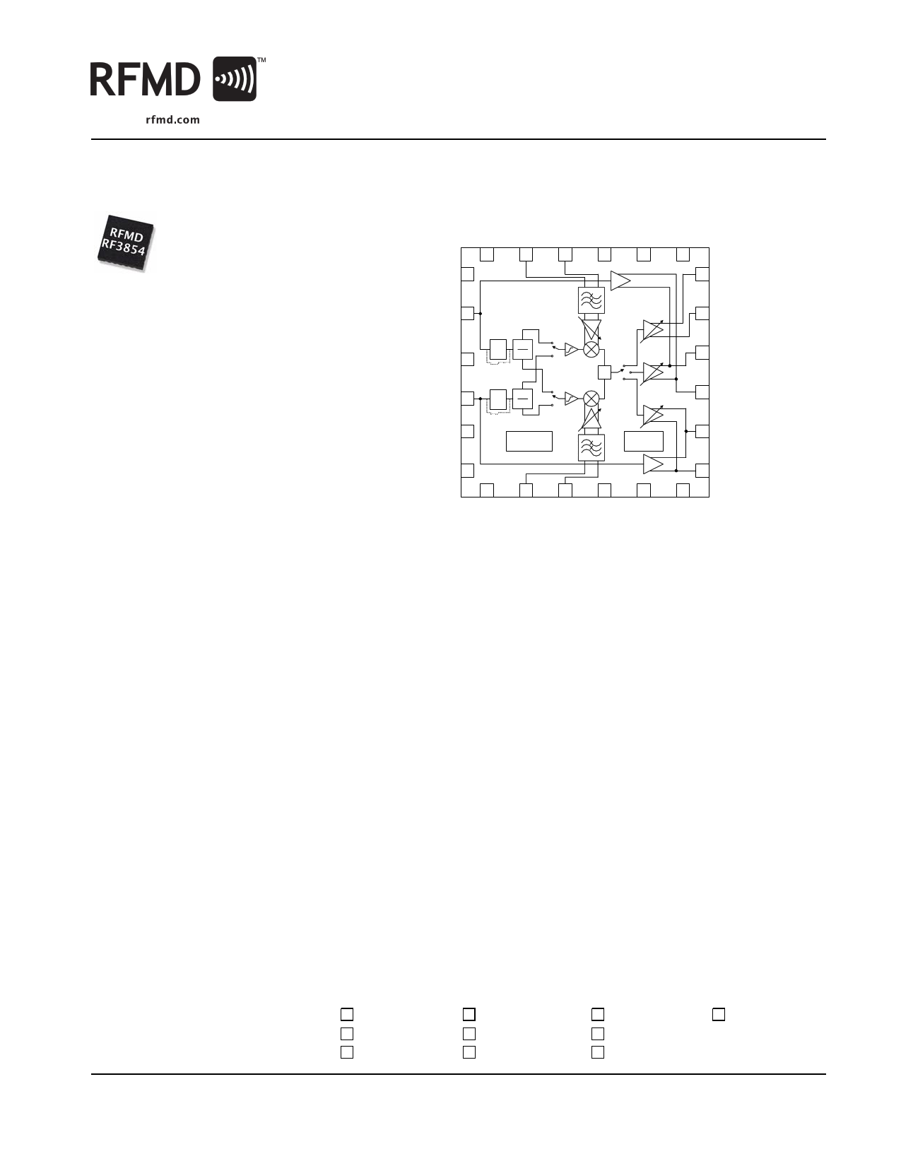
24 23 22
VCC2 1
LO HB P 2
Note: The die flag is the
chip's main ground.
LO HB N 3
DIV +45°
2 -45°
LO LB P 4
Flo +45°
x2 -45°
LO LB N 5
Mode Control
and Biasing
MODE C 6
789
21 20 19
18
RF OUT
WB P
17
RF OUT
WB N
16
RF OUT
HB P
Σ
15
RF OUT
HB N
Power
Control
14
RF OUT
LB P
13
RF OUT
LB N
10 11 12
Functional Block Diagram
Product Description
The RF3854 is a low noise, multi-mode, quad-band direct I/Q to RF modu-
lator and PA driver solution designed for digital modulation applications
ranging from 800MHz to 2000MHz. Frequency doublers, dividers and LO
buffers are included to support a variety of LO generation options.
Dynamic power control is supported through a single analog input giving
90dB of power control range for the W-CDMA mode and 40dB of power
control in the other two modes. Three sets of RF outputs are provided:
high band and low band low noise EDGE/GMSK outputs, as well as one
wideband W-CDMA output. The device is designed for 2.7V to 3.3V opera-
tion, and is assembled in a plastic, 24-pin, 4mmx4mm QFN.
Ordering Information
RF3854
RF3854PCBA-41X
Low Noise, Multi-Mode, Quad-Band, Quadrature Modulator
and PA Driver
Fully Assembled Evaluation Board
Optimum Technology Matching® Applied
GaAs HBT
9SiGe BiCMOS
GaAs pHEMT
GaN HEMT
GaAs MESFET
Si BiCMOS
Si CMOS
InGaP HBT
SiGe HBT
Si BJT
RF MICRO DEVICES®, RFMD®, Optimum Technology Matching®, Enabling Wireless Connectivity™, PowerStar®, POLARIS™ TOTAL RADIO™ and UltimateBlue™ are trademarks of RFMD, LLC. BLUETOOTH is a trade-
mark owned by Bluetooth SIG, Inc., U.S.A. and licensed for use by RFMD. All other trade names, trademarks and registered trademarks are the property of their respective owners. ©2006, RF Micro Devices, Inc.
Rev A1 DS070313
7628 Thorndike Road, Greensboro, NC 27409-9421 · For sales or technical
support, contact RFMD at (+1) 336-678-5570 or [email protected].
1 of 26
1 page 
RF3854
Parameter
General Conditions
Local Oscillator
LO LB Input Frequency
RF WB Output Frequency
Input Power
IQ Baseband Inputs
Min.
960
1920
-10.0
Specification
Typ. Max.
990
1980
0.0 +3.0
Unit
MHz
MHz
dBm
IQ Level
0.8
VP-P
IQ Common Mode
1.2
V
Input Bandwidth
8
11
MHz
Baseband Filter Attenuation 10
dB
Output Performance with CW Baseband Inputs
Wideband Mode
Mode=Wideband FLOx2 (see Control Logic Truth Table for Mode Control
Settings)
VGA and PA Driver
Output Power W-CDMA Modu-
5
dBm
lated*
Output Power CW
2
5
8 dBm
Gain Control Voltage Range 0.2
2.0 V
Gain Control Range
92
dB
Gain Control Slope
Modulator
Sideband Suppression
*
*
*
Carrier Suppression
3rd Harmonic of Modulation
Suppression at FC-3x300kHz
Spurious Outputs
73 dB/V
-48 -30 dBc
-50 -30 dBc
-50 -30 dBc
-50 -30 dBc
-42 -30 dBc
-41 -30 dBc
-38 -30 dBc
-23 -10 dBc
-55 -50 dBc
Spurious Output at Integer Multi-
ples of FLO LB*
FLO LB
4xFLO LB
6xFLO LB
Output Compression
-60.0
-14.0
-47.0
dBm
0 dBm
0 dBm
Output P1dB*
+11.5
dBm
* Not tested in Production
** Provides the same output power as modulated signal with associated crest factor.
Condition
3GPP W-CDMA
HQPSK, 1DPCCH+1DPDCH
Input IQ signal driven differentially and in
quadrature.
At 40MHz offset
VCC=2.7V, T=+25°C, LO=975MHz to
990MHz at -10dBm, IQ=540mVP-P** at
100kHz, unless otherwise noted
GC=2.0V, IQ=0.8VP-P at HQPSK
GC = 2.0 V
Difference between output power at GC=2.0V
and GC=0.2V
Calculated between GC=1.0V and 0.5V
GC=2.0V, No I/Q adjustment
GC=1.5V, No I/Q adjustment
GC=1.0V, No I/Q adjustment
GC=0.5V, No I/Q adjustment
GC=2.0V, No I/Q adjustment
GC=1.5V, No I/Q adjustment
GC=1.0V, No I/Q adjustment
GC=0.5V, No I/Q adjustment
GC = 2.0 V
GC=2.0V, I/Q=540mVP-P at 100kHz
FLO LB leakage
Second harmonic of carrier
Third harmonic of carrier
I/Q = 100 kHz
Rev A1 DS070313
7628 Thorndike Road, Greensboro, NC 27409-9421 · For sales or technical
support, contact RFMD at (+1) 336-678-5570 or [email protected].
5 of 26
5 Page 
RF3854
Parameter
Specification
Min. Typ. Max.
Unit
Condition
General Specifications
Operating Range
Supply Voltage 2.7
3.3 V
Temperature -40
+85 °C
Current Consumption
Refer to Logic Control Truth Table for Mode
Control Pin Voltages.
Sleep
<1 10 μA
Wideband FLOx1 (high power)
*
114
85
mA GC=2.0V
mA GC=0.2V
(medium power)
89
mA GC=2.0V
* 54
mA GC=0.2V
(low power)
63
mA GC=2.0V. See Note 1.
* 42
mA GC=0.2V. See Note 1.
Wideband FLOx2 (high power)
110
84
mA GC=2.0V
mA GC=0.2V
(medium power)
80
mA GC=2.0V
53 mA GC=0.2V
(low power)
54
mA GC=2.0V. See Note 1.
41 mA GC=0.2V. See Note 1.
High Band FLOx2
Low Band FLO/2
High Band Bypass
72
82
23
mA GC=2.0V
mA GC=2.0V
mA
Low Band Bypass
22
mA
Logic Levels
High Band FLOx1
Low Band FLOx1
76
74
mA GC=2.0V
mA GC=2.0V
Input Logic 0 0 0.4 V
Input Logic 1 1.4 VCC V
Logic Pins Input Current
<1.0
μA CMOS inputs
LO Input Ports
LO LB Input Frequency Range
800
1000
MHz
LO HB Input Frequency Range
1600
2000
MHz
Input Impedance
50 Ω Externally matched
Note 1: In low power mode it is recommended that the IQ level be reduced to 0.4VP-P. If IQ level is >0.4VP-P, this mode should be used for W-
CDMA TX power levels below -20dBm (measured at antenna).
Rev A1 DS070313
7628 Thorndike Road, Greensboro, NC 27409-9421 · For sales or technical
support, contact RFMD at (+1) 336-678-5570 or [email protected].
11 of 26
11 Page | ||
| Páginas | Total 26 Páginas | |
| PDF Descargar | [ Datasheet RF3854.PDF ] | |
Hoja de datos destacado
| Número de pieza | Descripción | Fabricantes |
| RF3854 | QUADRATURE MODULATOR AND PA DRIVER | RF Micro Devices |
| RF3855 | 3.1V LINEAR POWER AMPLIFIER | RF Micro Devices |
| RF3857 | DUAL CHANNEL LNA | RF Micro Devices |
| RF3858 | 3.0 V TO 4.2V ISM BAND TRANSMIT/RECEIVE MODULE | RF Micro Devices |
| Número de pieza | Descripción | Fabricantes |
| SLA6805M | High Voltage 3 phase Motor Driver IC. |
Sanken |
| SDC1742 | 12- and 14-Bit Hybrid Synchro / Resolver-to-Digital Converters. |
Analog Devices |
|
DataSheet.es es una pagina web que funciona como un repositorio de manuales o hoja de datos de muchos de los productos más populares, |
| DataSheet.es | 2020 | Privacy Policy | Contacto | Buscar |