|
|
|
PDF XR68C192 Data sheet ( Hoja de datos )
| Número de pieza | XR68C192 | |
| Descripción | (XR68C92 / XR68C192) DUAL UNIVERSAL ASYNCHRONOUS RECEIVER AND TRANSMITTER | |
| Fabricantes | Exar Corporation | |
| Logotipo | ||
Hay una vista previa y un enlace de descarga de XR68C192 (archivo pdf) en la parte inferior de esta página. Total 30 Páginas | ||
|
No Preview Available !
www.DataSheet4U.com
DESCRIPTION
XR68C92/192
DUAL UNIVERSAL ASYNCHRONOUS
RECEIVER AND TRANSMITTER
August 2005
The XR68C92/192 is a Dual Universal Asynchronous Receiver and Transmitter with 8 (XR68C92) / 16 (XR68C192)
bytes transmit and receive FIFO. The XR68C92/192 is a pin-to-pin compatible and an improved version of the
XR68C681 and the Philips SCC68692 UART with faster data access and other additional features. The operating
speed of the receiver and transmitter can be selected independently from a table of eighteen fixed baud rates, a
16X clock derived from a programmable counter/timer, or an external 1X or 16X clock. The baud rate generator
and counter/timer can operate directly from a crystal or from external clock input. The XR68C92/192 provides a
power-down mode in which the oscillator is stopped but the register contents are retained. The XR68C92/192 is
fabricated in an advanced CMOS process to achieve low power and high speed requirements.
FEATURES
Added features in devices with top marking of "D2" and
newer:
• 5 volt tolerant inputs
• Pin to pin compatible and improved version of the
SCC68692 and XR68C681
• Enhanced Multidrop mode operation with separate
storage for address and data tags (9th bit)
• 8 Bytes transmit/receive FIFO (XR68C92)
•16 Bytes transmit/receive FIFO (XR68C192)
• Standard baud rates from 50bps to 230.4kbps
• Non-standard baud rate of up to 1Mbps
• Transmit and Receive trigger levels
• Watch dog timer
• Programmable clock source for receiver and trans-
mitter of each channel
• Single interrupt output
• 7 Multipurpose inputs, 8 Multipurpose outputs
• 2.97 to 5.5 volt operation
• Programmable character lengths (5, 6, 7, 8)
• Parity, framing, and over run error detection
• Programmable 16-bit timer/counter
• On-chip crystal oscillator
• Power down mode
ORDERING INFORMATION
A3 7
IP0 8
R/-W 9
-DTACK 10
RXB 11
N.C. 12
TXB 13
OP1 14
OP3 15
OP5 16
OP7 17
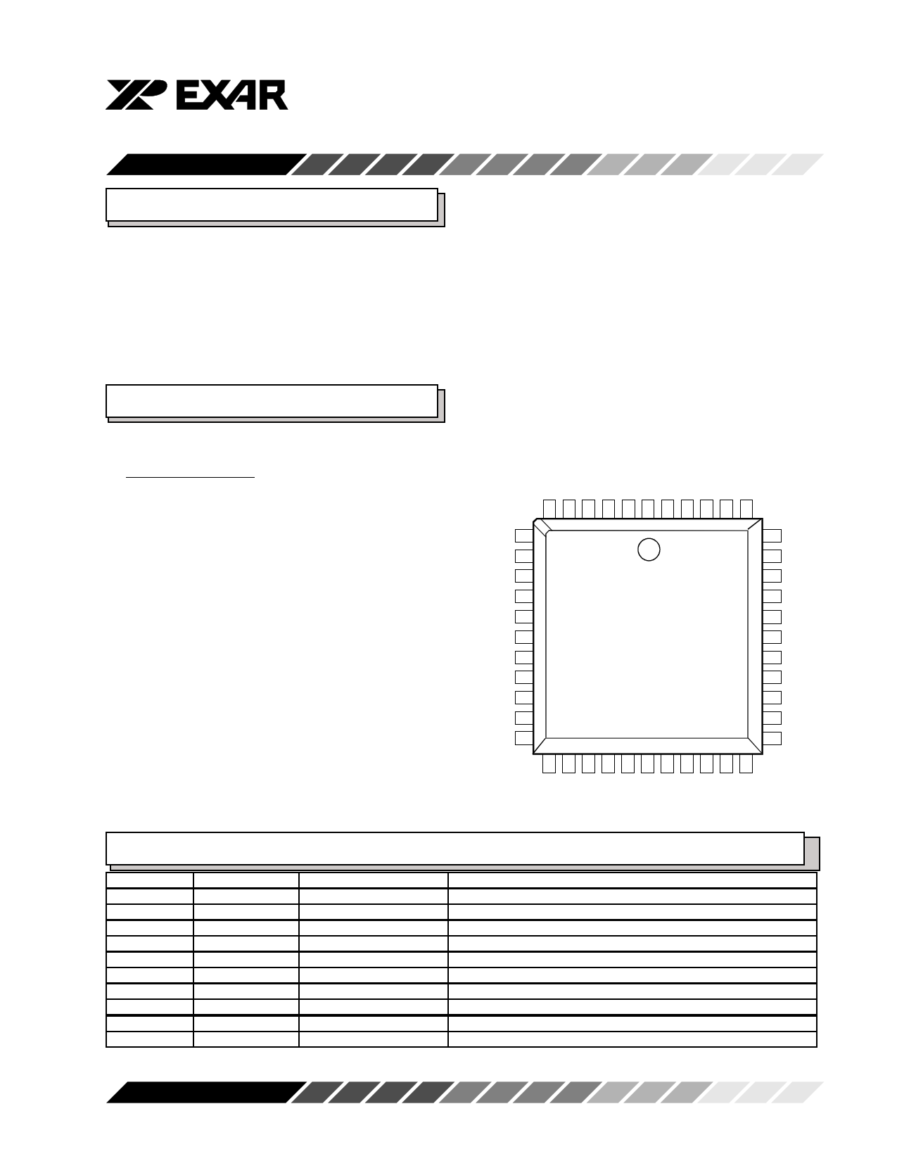
PLCC Package
XR68C92
XR68C192
39 -CS
38 -RESET
37 XTAL2
36 XTAL1
35 RXA
34 N.C.
33 TXA
32 OP0
31 OP2
30 OP4
29 OP6
Part number Package
XR68C92CP 40-Lead PDIP
XR68C92CJ 44-Lead PLCC
XR68C92CV 44-Lead LQFP
XR68C92IP 40-Lead PDIP
XR68C92IJ 44-Lead PLCC
XR68C92IV 44-Lead LQFP
XR68C192CJ 44-Lead PLCC
XR68C192CV 44-Lead LQFP
XR68C192IJ 44-Lead PLCC
XR68C192IV 44-Lead LQFP
Operating temperature Device Status
0° C to + 70° C
Active. See the XR68C92CV for new designs.
0° C to + 70° C
Active
0° C to + 70° C
Active
-40° C to + 85° C
Active. See the XR68C92IV for new designs.
-40° C to + 85° C
Active
-40° C to + 85° C
Active
0° C to + 70° C
Active
0° C to + 70° C
Active
-40° C to + 85° C
Active
-40° C to + 85° C
Active
Rev. 1.33
EXAR Corporation, 48720 Kato Road, Fremont, CA 94538 • (510) 668-7000 • FAX (510) 668-7017
1 page 
XR68C92/192
SYMBOL DESCRIPTION (* 44 pin LQFP)
Symbol
XTAL2
RXA, RXB
TXA, TXB
IP0
IP1
IP2
IP3
IP4
IP5
OP0
OP1
OP2
Pin Signal
44 40 44* type
Pin Description
37 33 31 O Crystal input 2 or buffered clock output. See XTAL1.
35,11 31,10 29,5
I Serial data input. The serial information (data) received from
serial port to XR68C92/192 receive input circuit. A mark
(high) is logic one and a space (low) is logic zero.This input
must be held at logic one when idle and during power down.
33,13 30,11 28,6 O Serial data output. The serial data is transmitted via this pin
with additional start , stop and parity bits. This output will be
held in mark (high) state during reset, local loop back mode
or when the transmitter is disabled.
8 7 2 I Multi-purpose input or Channel A Clear-To-Send (-CTSA
active low). If not used, this pin should be tied to VCC.
5 4 43 I Multi-purpose input or Channel B Clear-To-Send (-CTSB
active low). If not used, this pin should be tied to VCC.
40 36 34
I Multi-purpose input or Channel B receive external clock
input (received data is sampled on the rising edge of the
clock) or Timer/Counter External clock input. If not used, this
pin should be tied to VCC or GND.
3 2 41 I Multi-purpose input or Channel A transmit external clock
input. The transmit data is clocked on the falling edge of the
clock. If not used, this pin should be tied to VCC or GND.
43 39 37
I Multi-purpose input or Channel A receive external clock
input. The received data is clocked on the rising edge of the
clock. If not used, this pin should be tied to VCC or GND.
42 38 36
I Multi-purpose input or Channel B transmit external clock
input. The transmit data is clocked on the falling edge of the
clock. If not used, this pin should be tied to VCC or GND.
32 29 27 O Multi-purpose output. General purpose output or Channel A
Request-To-Send (-RTSA active low).
14 12
7
O Multi-purpose output. General purpose output or Channel B
Request-To-Send (-RTSB active low).
31 28 26 O Multi-purpose output. General purpose output or one of the
Rev. 1.33
5
5 Page 
XR68C92/192
or the FIFO-full status bits can be selected to cause an
interrupt (see MR1A, MR1B bit-6).
In addition to the data byte, three status bits (parity
error, framing error, and received break) are appended
to each data character in the FIFO (overrun is not). By
programming the error-mode control bit (MR1A, MR1B
bit-5), status can be provided for “character” or “block”
modes. In the “character” mode, the status register
(SRA, SRB) is updated on a character-by-character
basis and applies only to the character at the top of the
FIFO. Thus, the status must be read before the char-
acter is read. Reading the character pops the data byte
and its error flags off the FIFO. In the “block” mode, the
status provided in the status register for the parity error,
framing error, and received-break conditions are the
logical OR of these respective bits, for all the data bytes
in the FIFO stack since the last reset error command
(see CRA, CRB bits 7:4) was issued. That is, beginning
immediately after the last reset-error command was
issued, a continuous logical-OR function of corre-
sponding status bits is produced in the status register
as each character enters the FIFO.
The block mode is useful in applications requiring the
exchange of blocks of information where the software
overhead of checking each character's error flags
cannot be tolerated. In this mode, entire messages can
be received and only one data integrity check is per-
formed at the end of each message. Although data
reception in this manner has speed advantages, there
are also disadvantages. If an error occurs within a
message the error will not be recognized until the final
check is performed. Also, there is no indication of
which character(s) is in error within the message.
Reading the status register (SRA, SRB) does not affect
the FIFO. The FIFO is “popped” only when the receive
buffer is read. If the FIFO is full when a new character
is received, that character is held in the receive shift
register until a FIFO position is available. If an addi-
tional character is received while this state exists, the
contents of the FIFO are not affected, but the character
previously in the shift register is lost and the overrun-
error status bit will be set upon receipt of the start bit of
the new overrunning character.
To support flow control, a receiver can automatically
negate and reassert the request-to-send (RTS) output
(RX RTS control - see MR1A, MR1B bit-7). The re-
quest-to-send output (at OP0 or OP1 for channel A or
B respectively) will automatically be negated by the
receiver when a valid start bit is received and the FIFO
stack is full. When a FIFO position becomes available,
the request-to-send output will be reasserted auto-
matically by the receiver. Connecting the request-to-
send output to the clear-to send (CTS) input of a
transmitting device prevents overrun errors in the
receiver. The RTS output must be manually asserted
the first time. Thereafter, the receiver will control the
RTS output.
If the FIFO stack contains characters and the receiver
is then disabled, the characters in the stack can still be
read but no additional characters can be received until
the receiver is again enabled. If the receiver is disabled
while receiving a character, or while there is a charac-
ter in the shift register waiting for a FIFO opening, these
characters are lost. If the receiver is reset, the FIFO
stack and all of the receiver status bits, the correspond-
ing output ports, and the interrupt request are reset. No
additional characters can be received until the receiver
is again enabled.
LOOPBACK MODES
Besides the normal operation mode in which the re-
ceiver and transmitter operate independently, each
XR68C92/192 channel can be configured to operate in
various looping modes (see MR2A, MR2B bits 7:6) that
are useful for local and remote system diagnostic
functions.
AUTOMATIC ECHO MODE
In this mode, the channel automatically retransmits the
received data on a bit-by-bit basis. The local CPU-to-
receiver communication continues normally but the
CPU-to-transmitter link is disabled.
LOCAL LOOPBACK MODE
In this mode, the transmitter output is internally con-
nected to the receiver input. The external TX pin is held
in the mark (high) state in this mode. By sending data
to the transmitter and checking that the data as-
sembled by the receiver is the same data that was sent,
proper channel operation can be assured. In this mode
the CPU-to-transmitter and CPU-to-receiver commu-
nications continue normally.
REMOTE LOOPBACK MODE
In this mode, the channel automatically retransmits the
received data on a bit-by-bit basis. The local CPU-to-
receiver and CPU-to-transmitter links are disabled.
Rev. 1.33
11
11 Page | ||
| Páginas | Total 30 Páginas | |
| PDF Descargar | [ Datasheet XR68C192.PDF ] | |
Hoja de datos destacado
| Número de pieza | Descripción | Fabricantes |
| XR68C192 | (XR68C92 / XR68C192) DUAL UNIVERSAL ASYNCHRONOUS RECEIVER AND TRANSMITTER | Exar Corporation |
| Número de pieza | Descripción | Fabricantes |
| SLA6805M | High Voltage 3 phase Motor Driver IC. |
Sanken |
| SDC1742 | 12- and 14-Bit Hybrid Synchro / Resolver-to-Digital Converters. |
Analog Devices |
|
DataSheet.es es una pagina web que funciona como un repositorio de manuales o hoja de datos de muchos de los productos más populares, |
| DataSheet.es | 2020 | Privacy Policy | Contacto | Buscar |